
Interactive electronics resource
RTL Kit Range Instructions
Build, understand and experiment with the RTL Kit Range. This resource brings the original kit material into the current MitchElectronics format with the schematic, circuit explanation, component and PCB information, construction guidance, troubleshooting and practical ideas where available.
Introduction
What is the RTL Kit Range?
The RTL Kit range are discrete logic boards that teach how RTL logic gates work. With integrated buttons and LEDs, each kit can be used independently to learn about a specific logic function, such as AND and OR, while also allowing for combined use with other RTL kits, realising more complex logic functions.
Even though RTL is no longer found in modern day electronics, it demonstrates some features that are indeed still use, such as NMOS logic, open collectors, and transistor amplifiers. By making the kit discrete (i.e. no integrated circuits) you can see how components that go into modern semiconductors are used to power our world.
Pre-learning – The Logic Board
Before diving into the RTL kits, it might be a good idea to get yourself the Logic Board and read through its instructions, as it teaches about logic and binary, both of which are needed to understand this kit.
What is RTL?
RTL stands for Resistor Transistor Logic, which itself is what’s known as a logic family. All logic families and logic gates operate on binary, being 1’s and 0s, but how these logic families achieve this can vary greatly.
An analogy to this concept could be something like signalling over long distances. You could either use smoke signals, large flags, or a bright source of light to all transmit a binary signal over great distances, but no matter what method you choose, they all send binary,
In the case of logic families, some may use current, others will use voltage, and even those using voltage will all have different voltage levels. Furthermore, how those logic families generate those currents and/or voltages can also greatly different, as we will see in the RTL gates.
For example, CMOS logic (the most common type today, and also the simplest), uses two transistors in a push-pull configuration to connect an output to either power or ground, whereas in TTL logic (widely used in the 1970s-1980s), used a combination of overly complex BJT transistor emitters as inputs, which honestly, still doesn’t make sense.
Schematic
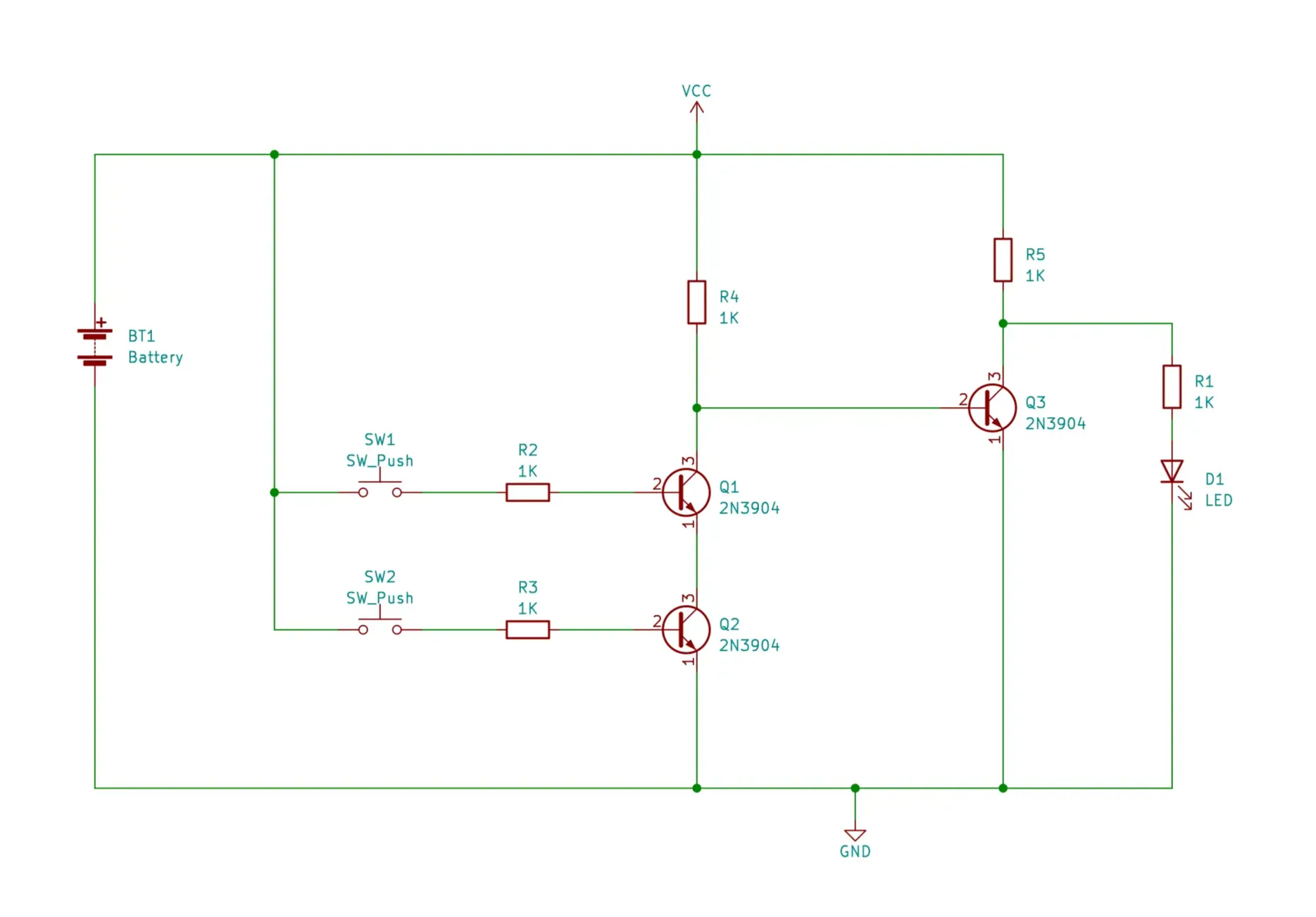
RTL AND
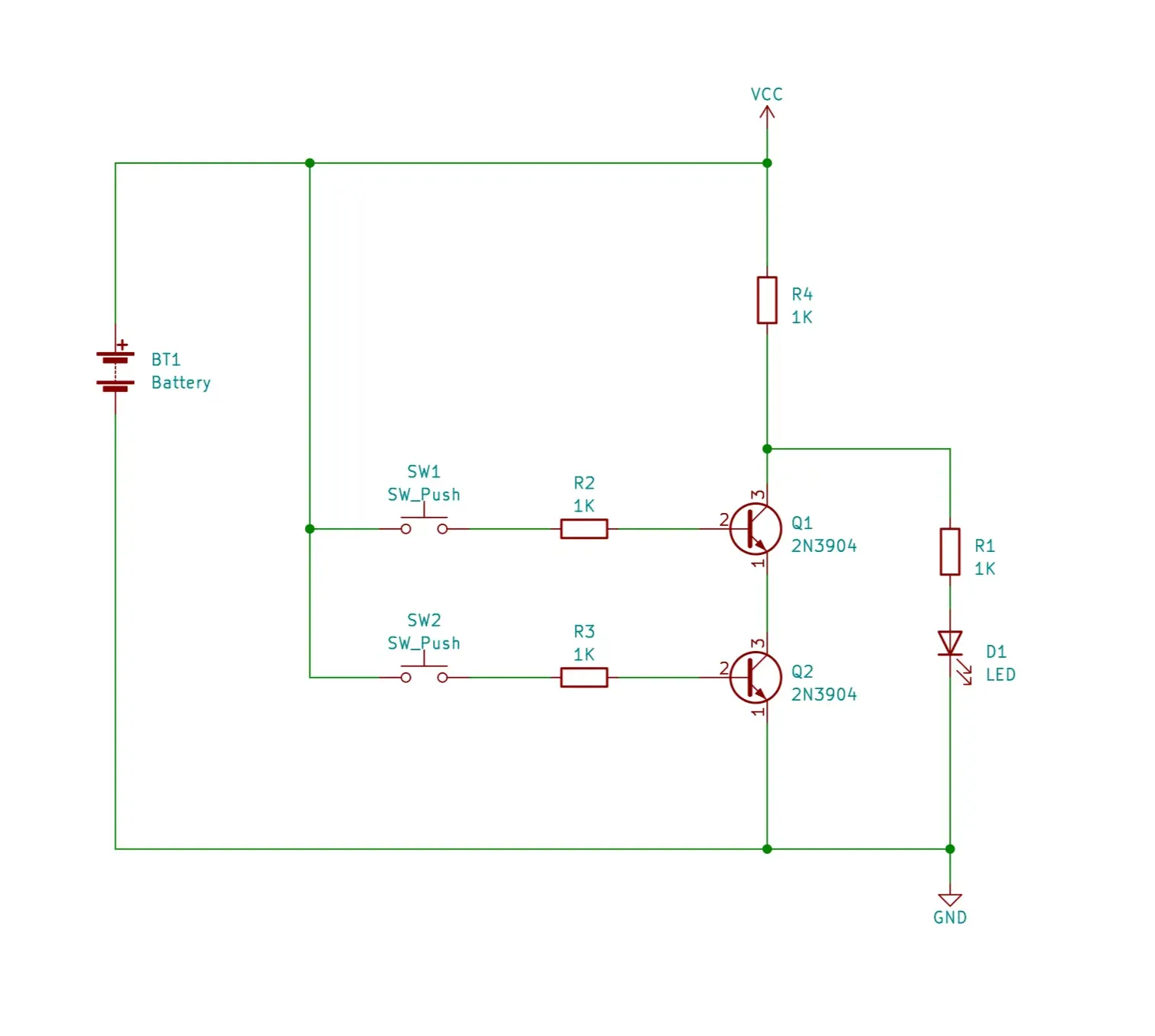
RTL NAND
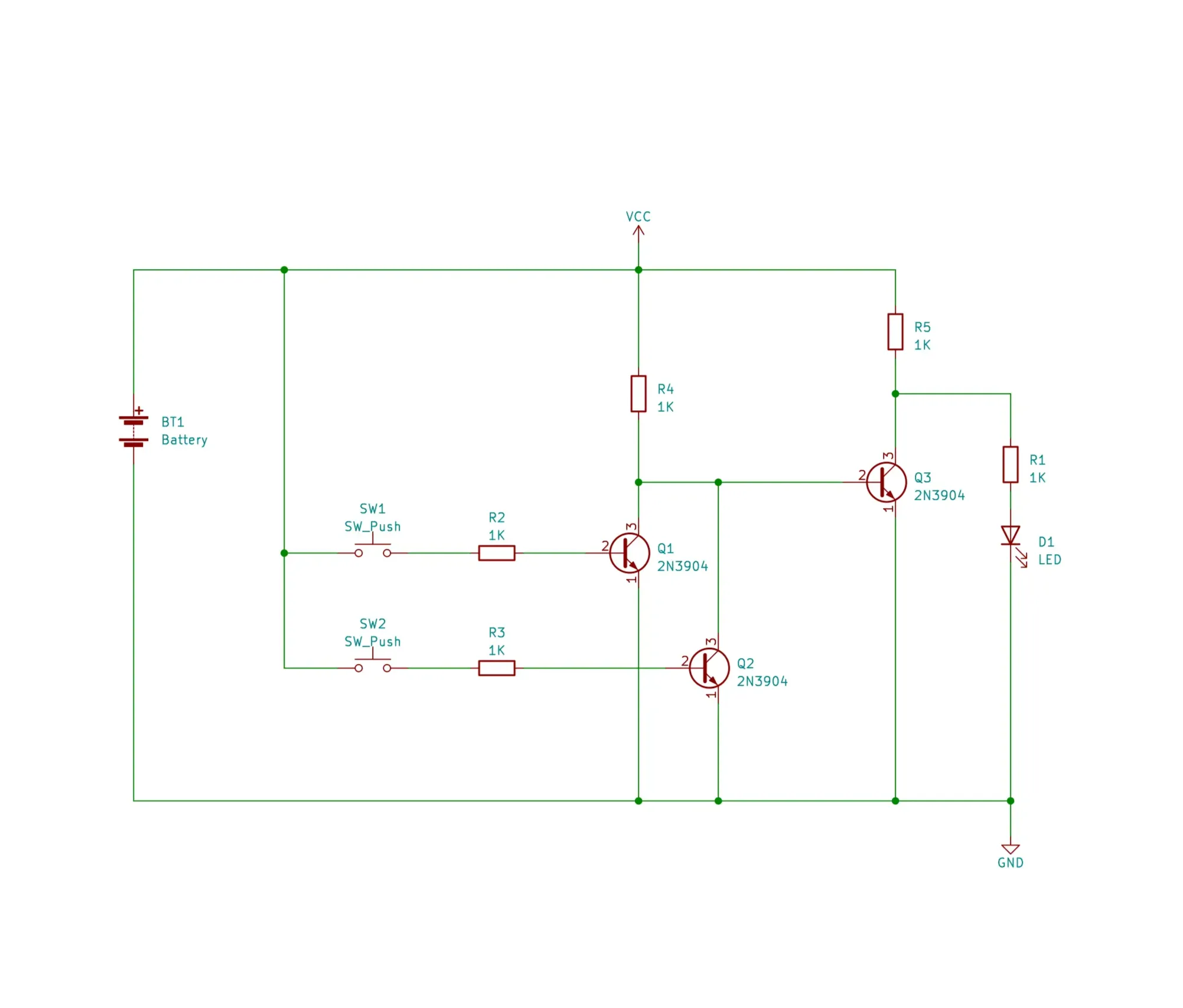
RTL OR
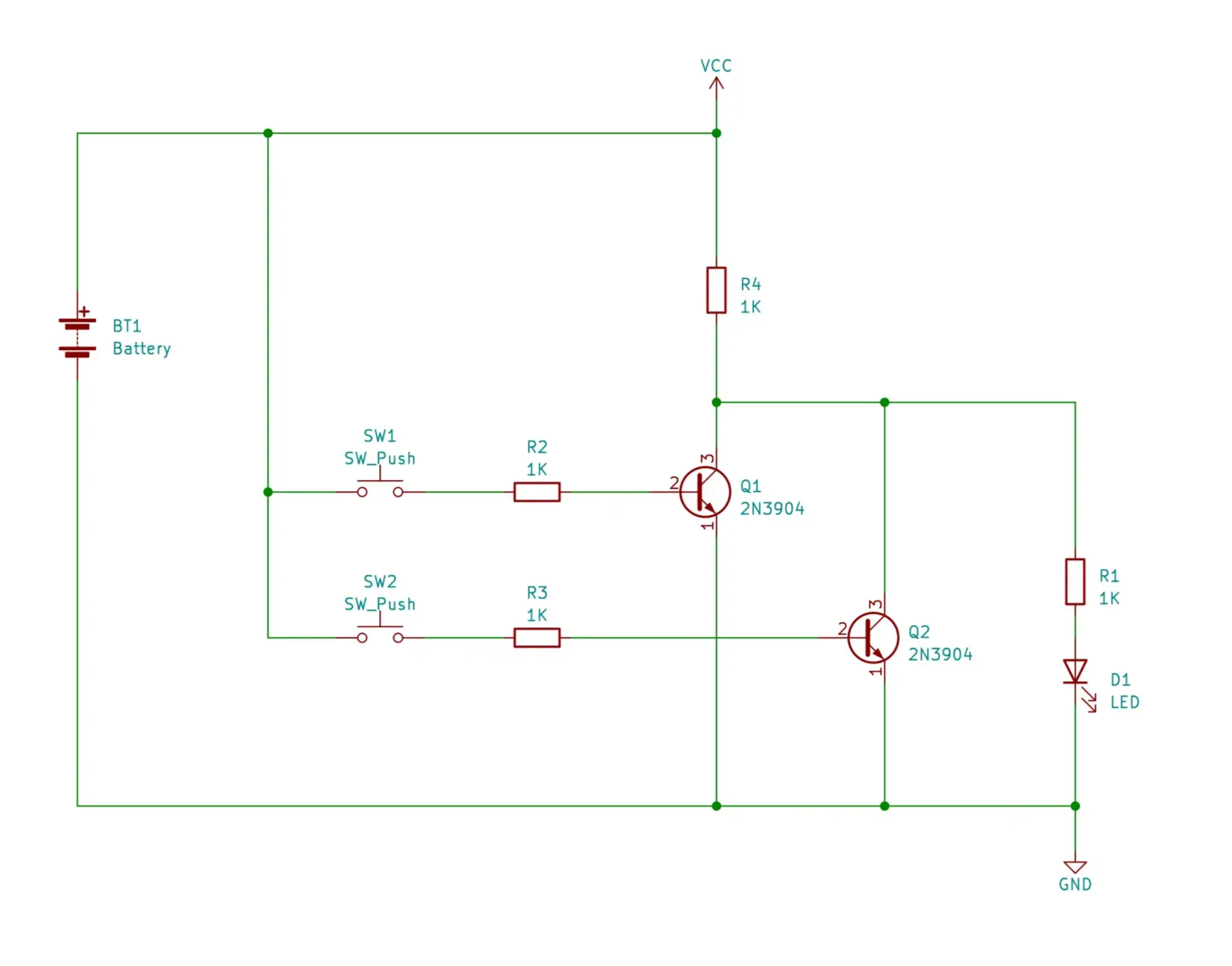
RTL NOR
RTL NOT
How does RTL work?
The RTL NOT Gate
To understand how RTL logic gates work, its best to start with the most basic one, the NOT gate.
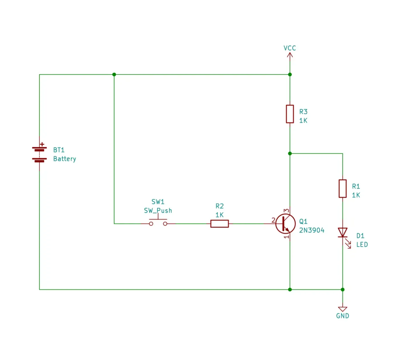
A NOT gates output will always be the opposite to its input, with an input of 1 becoming a 0, and vice versa. The input to the RTL NOT gate, as shown in the schematic, is controlled by the switch SW1, and the LED D1 indicates the output of the NOT gate.
When the switch is unpressed, there is no current flowing into the RTL NOT gate, meaning that the input is a logical 0. Because there is no current flowing into the transistor Q1, it cannot conduct electricity, meaning that current can flow through R3, through R1, and then through the LED, turning it on. Because the LED is on, this shows that the output (the collector of Q1) is VCC, representing a logical 1.
If we then push the switch, current can flow into Q1 via R2, and this represents an input of 1. Because the transistor is fully saturated (i.e. becomes fully conductive), it means that all the current coming through R3 is shorted to ground through the transistor. As such, no current is allowed to flow through the LED, turning it off, thus representing a logic 0.
The RTL NAND Gate
The RTL NAND Gate uses two transistors in series to realize the NAND function. A NAND gate’s output is only off when both inputs are on. By examining the schematic, we can see how this works.
If neither input is on, neither Q1 nor Q2 are conducting, allowing the output LED to turn on as current flows through R4, R1, and D1. If one transistor is turned on while the other remains off, the path to ground via the transistors is incomplete. As a result, the current still flows through the LED circuit, keeping the LED on.
The RTL NOR Gate
The RTL NOR Gate also uses two transistors, but instead of being in series, they are arranged in parallel. This means that if either transistor is on (or both), there is a path between the output and ground, making the output 0. However, if neither input is on, there is no path from the output to ground, resulting in an output of 1.
The Other Gates
The other gates in the series, the AND and OR gates, are created by adding a NOT gate to the output of the NAND and NOR gates, respectively.
But can you spot a pattern with the RTL kits?
- Every input has its own transistor.
- AND functions are achieved by placing transistors in series, as all need to be on (1 AND 2 AND 3, etc.).
- OR functions are achieved by placing transistors in parallel, as only one needs to be on for the output to be set (1 OR 2 OR 3).
Multi-input logic gates, such as 4-input AND or OR gates, can be created by adding more transistors. For AND gates, more transistors are placed in series, while for OR gates, additional transistors are placed in parallel.
What Problems Does RTL Introduce?
RTL takes advantage of transistors essentially pulling current away from some output circuit. While this is straightforward to implement, it also introduces several significant challenges.
The first issue with RTL is that current is always flowing (either through the output or directly to ground), making it very energy-intensive. While this is not a major issue for a few gates, it becomes problematic when thousands of these gates are integrated into a tiny silicon chip. The energy consumption can generate enough heat to cause the chip to become very hot.
The second issue is that with such high current consumption, RTL cannot be scaled up to billions of transistors. For comparison, NMOS (a closely related logic family) CPUs in the 1980s could consume a few watts of power with around 10,000 transistors. A modern GPU, if built with RTL, would require hundreds of kilowatts of power, making it impractical.
The third issue is that RTL gates using BJTs (Bipolar Junction Transistors) are relatively slow, making them unsuitable for high-speed logic. Increasing the size of the collector resistor (e.g., R3 in the NOT gate) can reduce current consumption, but this comes at the cost of even slower speeds.
This slow speed also causes issues in complex gates with multiple transistors, as it takes time for each transistor to turn on. This can lead to unexpected outputs that rapidly change as signals propagate through the circuit.
Try it yourself
Circuit simulation
What you need
Component List
Inspect the board
Interactive BOM
Board reference
PCB & assembly
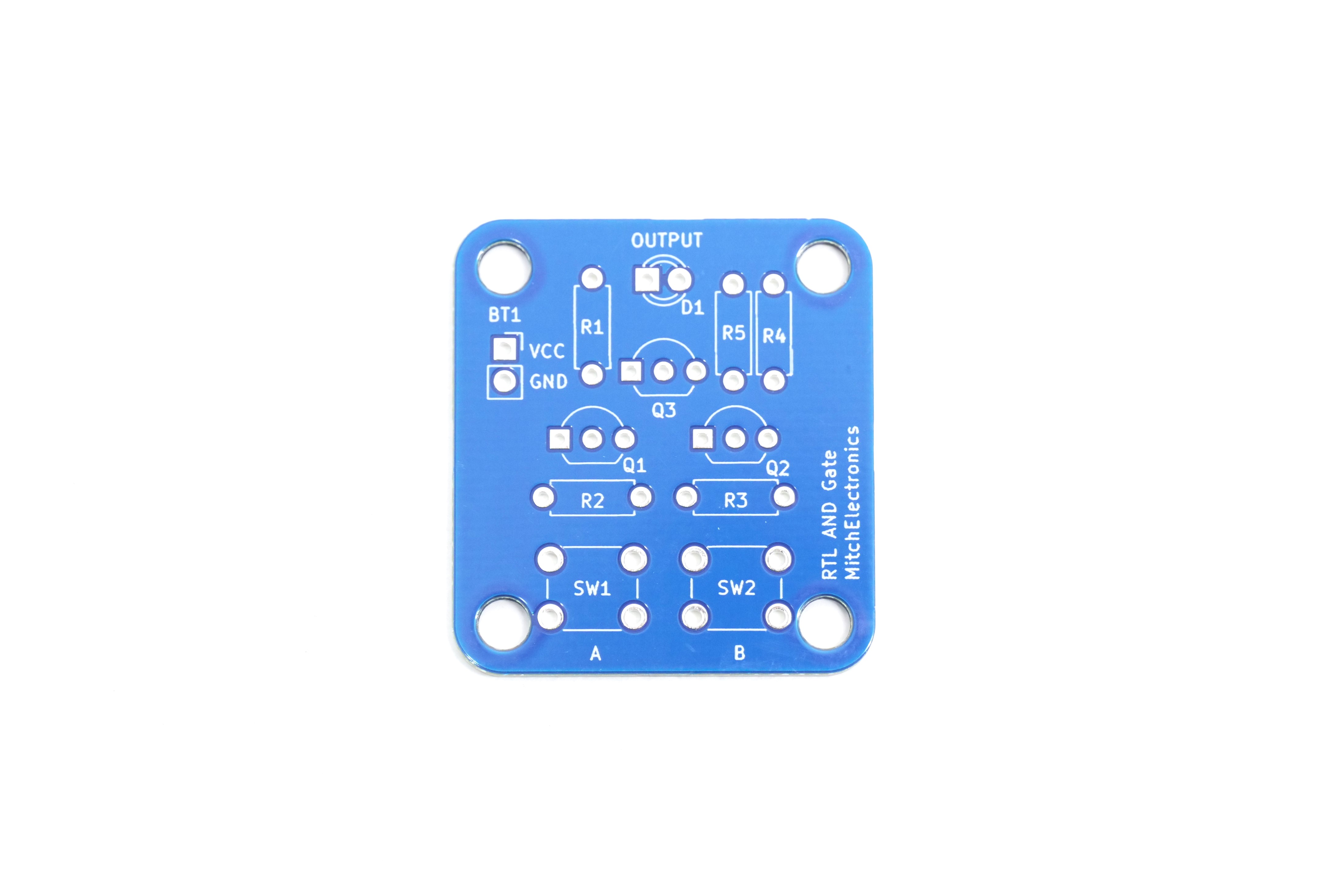
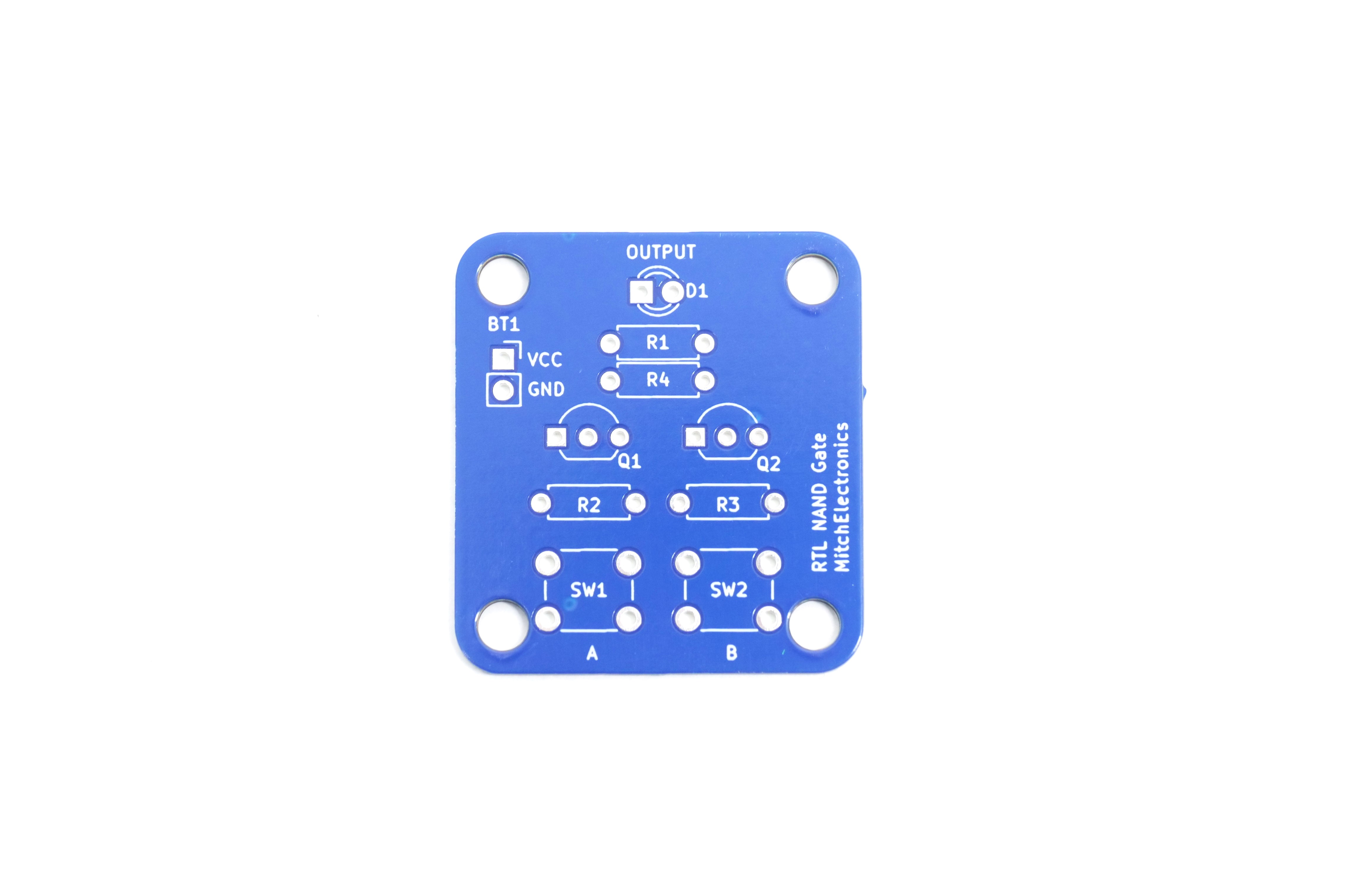
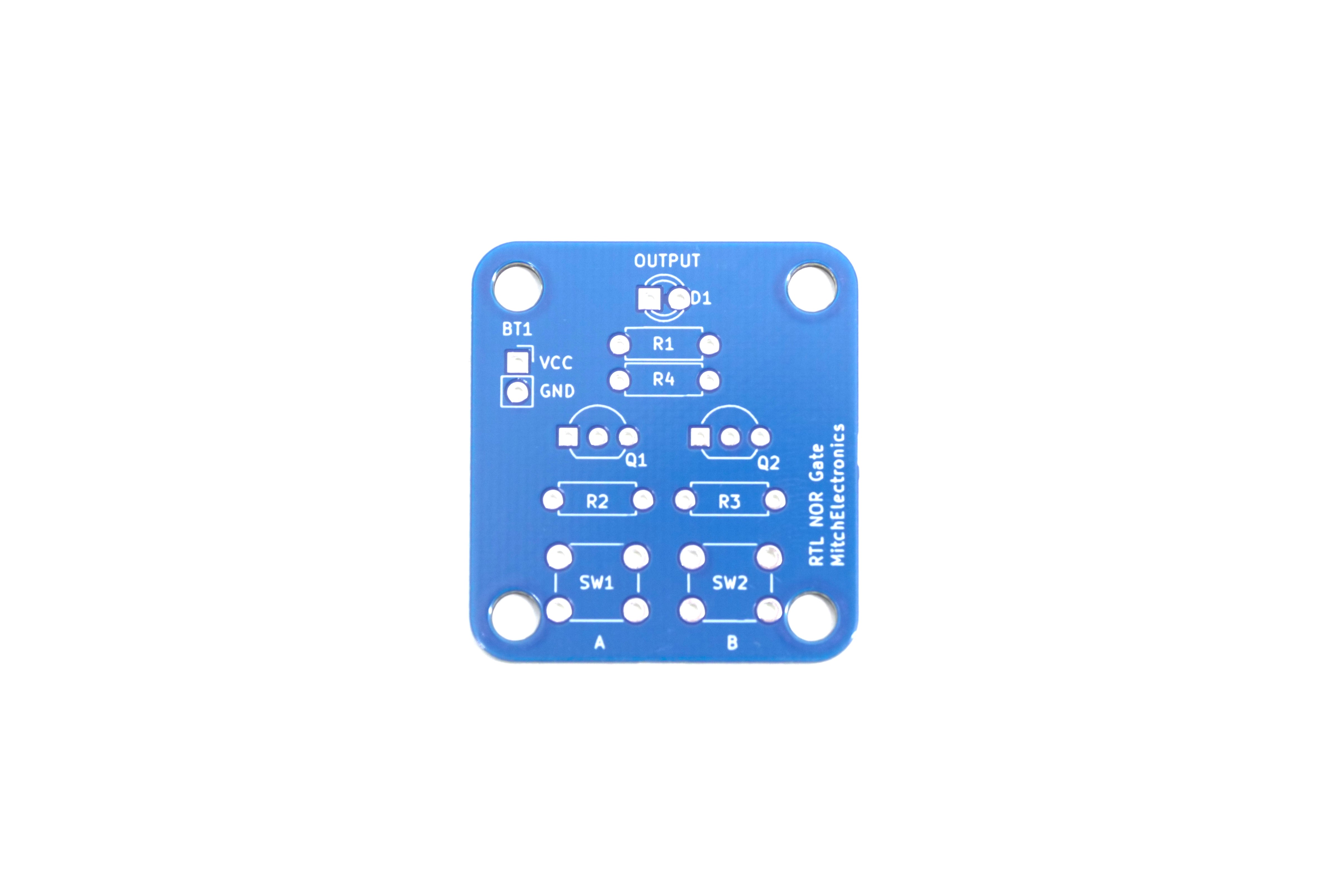
The PCB silkscreen and component references should be checked against the component list before soldering each part.
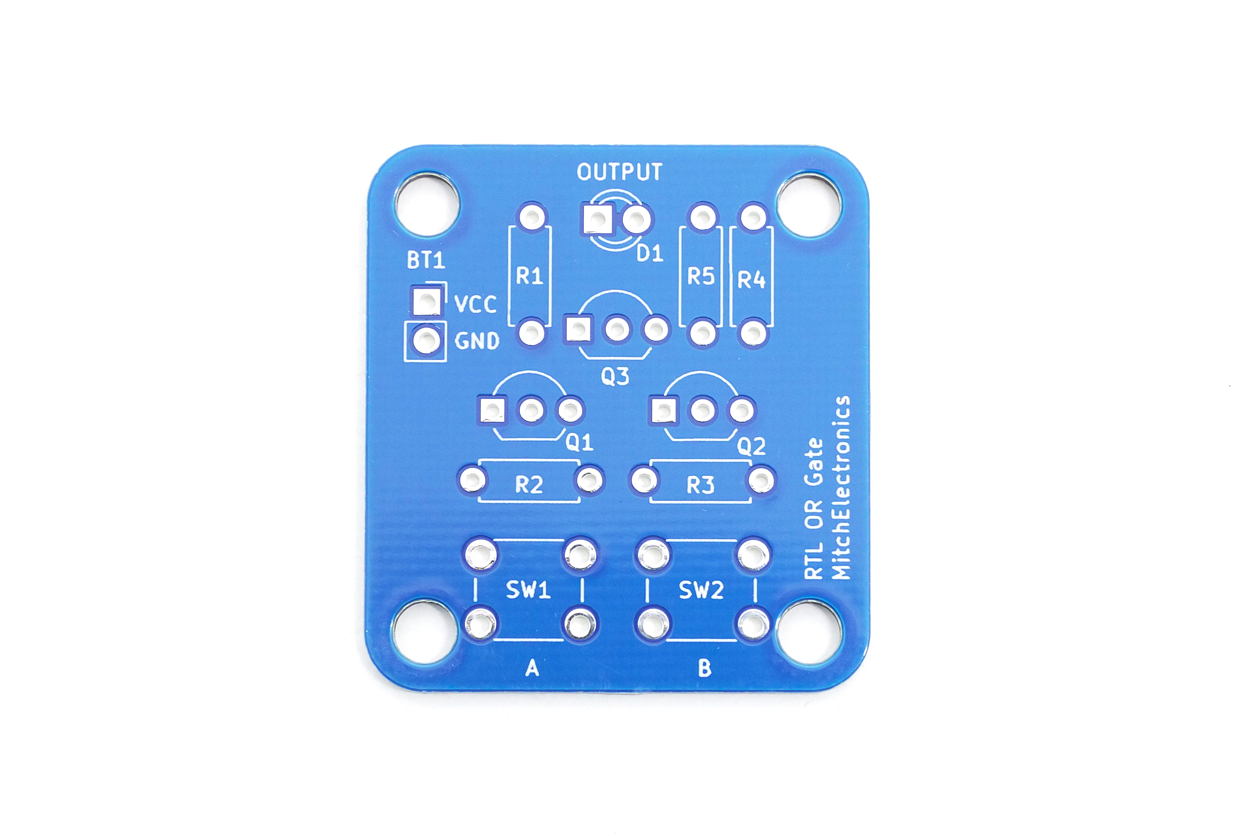
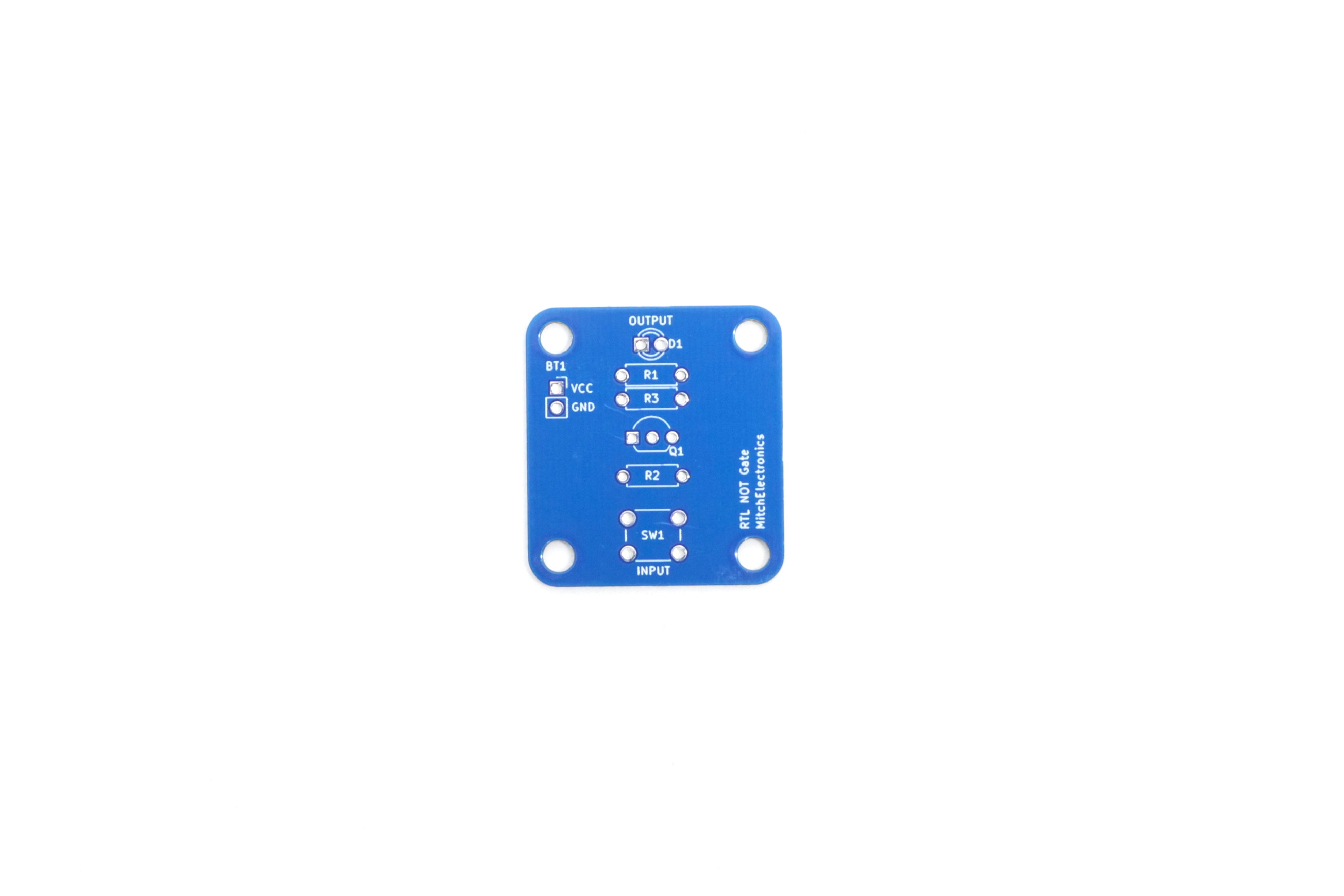
Before applying power
- Check every component against its PCB reference.
- Confirm the orientation of all polarised components and ICs.
- Inspect for solder bridges, unsoldered pads and clipped leads that could cause a short.
- Check that no loose wire or solder debris remains on the board.
Build with confidence
Construction tips
Recommended build order
A reliable way to assemble RTL Kit Range is to work from the lowest-profile components to the tallest. This keeps the PCB easy to access while you solder.
- Fit resistors, links and other low-profile components first.
- Fit small capacitors and diodes, checking polarity where applicable.
- Fit IC sockets and small semiconductors, observing the orientation markings.
- Fit larger capacitors, potentiometers, switches and other controls.
- Fit LEDs, connectors and the remaining taller components.
- Insert socketed ICs only after soldering around the socket is complete.
- Inspect every joint and check for solder bridges before applying power.
Electronics construction guidance
If you are new to kit construction, use the Soldering Guide alongside these instructions. Identify each component before fitting it and compare its reference with the component list and PCB silkscreen.
When it does not work
Troubleshooting
Nothing happens when power is applied
- Confirm the supply is connected to the correct input and with the correct polarity.
- Check that ICs, diodes, LEDs, transistors and electrolytic capacitors are fitted in the correct orientation.
- Compare component values and positions against the component list and PCB reference.
- Inspect for missed joints, dry joints and accidental solder bridges.
The circuit powers up but does not behave as expected
This kit is intended for resistor-transistor logic gate experiments. If the output is stuck, unstable or outside the expected behaviour, use the schematic to trace the circuit a stage at a time rather than replacing several parts at once.
Check the components around the part of the circuit responsible for the output or timing first. A misplaced resistor, reversed semiconductor or poor connection can allow a circuit to power up while preventing it from operating correctly.
The circuit works intermittently
Intermittent behaviour is often caused by a marginal solder joint, a loose connector or a component lead that has not been fully soldered. Gently inspect the board with power removed and reflow any joint that looks dull, cracked or incomplete.
If the fault remains, compare the assembled board with the schematic and PCB reference one connection at a time.
Ready to test and experiment?
Feeling brave? Consider using different resistor values Attach these gates to other circuits to make more complex logic systems
Once the board is working, compare its behaviour with the schematic and the explanation above. Try changing only one input, control or permitted component value at a time so you can clearly see what effect that change has on the circuit.