RP2040 at the centre
Dual Cortex-M0+ cores, 264KB of SRAM and the flexible RP2040 peripheral system provide considerably more headroom than traditional 8-bit Uno-class boards.

RP2040 development hardware
RP-Duino combines Raspberry Pi's RP2040 microcontroller with the familiar Arduino Uno form factor and a board-level interface designed to work with both modern 3.3V electronics and existing 5V hardware.
Why RP-Duino?
The RP2040 is a capable modern microcontroller, but many established shields, sensors and modules still expect 5V logic. RP-Duino adds the interface circuitry needed to make those two worlds easier to combine.
Dual Cortex-M0+ cores, 264KB of SRAM and the flexible RP2040 peripheral system provide considerably more headroom than traditional 8-bit Uno-class boards.
Board-level translation sits between the RP2040's 3.3V GPIO and the external headers, reducing the amount of separate level-shifting hardware needed in many 5V projects.
The 68.6mm × 53.4mm board follows the Arduino Uno form factor, making it easier to reuse existing mechanical layouts and compatible add-on hardware.
USB-C provides programming, data and power, while a 12V barrel-jack input supports projects that need a more traditional external supply.
Board specification
The board keeps the RP2040's processing capability while adding the voltage translation, controls and connectors needed for a more flexible development platform.
| Microcontroller | RP2040, dual-core Arm Cortex-M0+ |
|---|---|
| CPU frequency | Up to 133MHz |
| SRAM | 264KB |
| Flash | 4MB external flash |
| Digital GPIO | 19 × 5V-tolerant I/O |
| Analogue inputs | 4 × 5V-tolerant inputs |
| User buttons | 2 × GPIO buttons, independent of the main headers |
| User LEDs | 4 × GPIO LEDs, independent of the main headers |
| Programming controls | Reset and firmware/boot switches |
| USB | USB-C for connectivity and power |
| External power | 12V DC barrel jack |
| Form factor | Arduino Uno footprint |
| Dimensions | 68.6mm × 53.4mm |
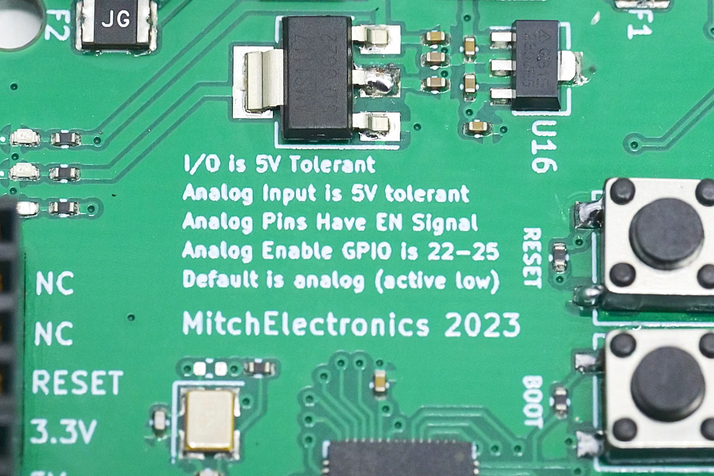
The level-shifting network changes the available source/sink behaviour and switching characteristics. Design loads around the board interface rather than assuming normal RP2040 GPIO drive capability.
The reason for the board
3.3V logic is now common, but electronics has decades of 5V hardware behind it. The problem becomes obvious when a modern controller has to connect directly to older shields, modules, interfaces or laboratory hardware.
A standard RP2040 design is based around 3.3V I/O. That is a good match for many current sensors and ICs, but a 5V signal cannot simply be treated as a safe RP2040 input. External translation or conditioning is normally required whenever the surrounding hardware uses a higher logic voltage.
That extra circuitry is perfectly reasonable in a purpose-built product, but it becomes inconvenient on a development board intended to replace or coexist with older Uno-style hardware. It adds components, wiring, board area and another place for a prototype to go wrong.
RP-Duino moves much of that translation onto the development board itself. The goal is not to make voltage domains disappear, but to make mixed-voltage prototyping more practical.
Useful when working with
Digital translation
Each translated digital channel uses a BSS138 MOSFET level-shifting arrangement between the RP2040 side and the external 5V side.
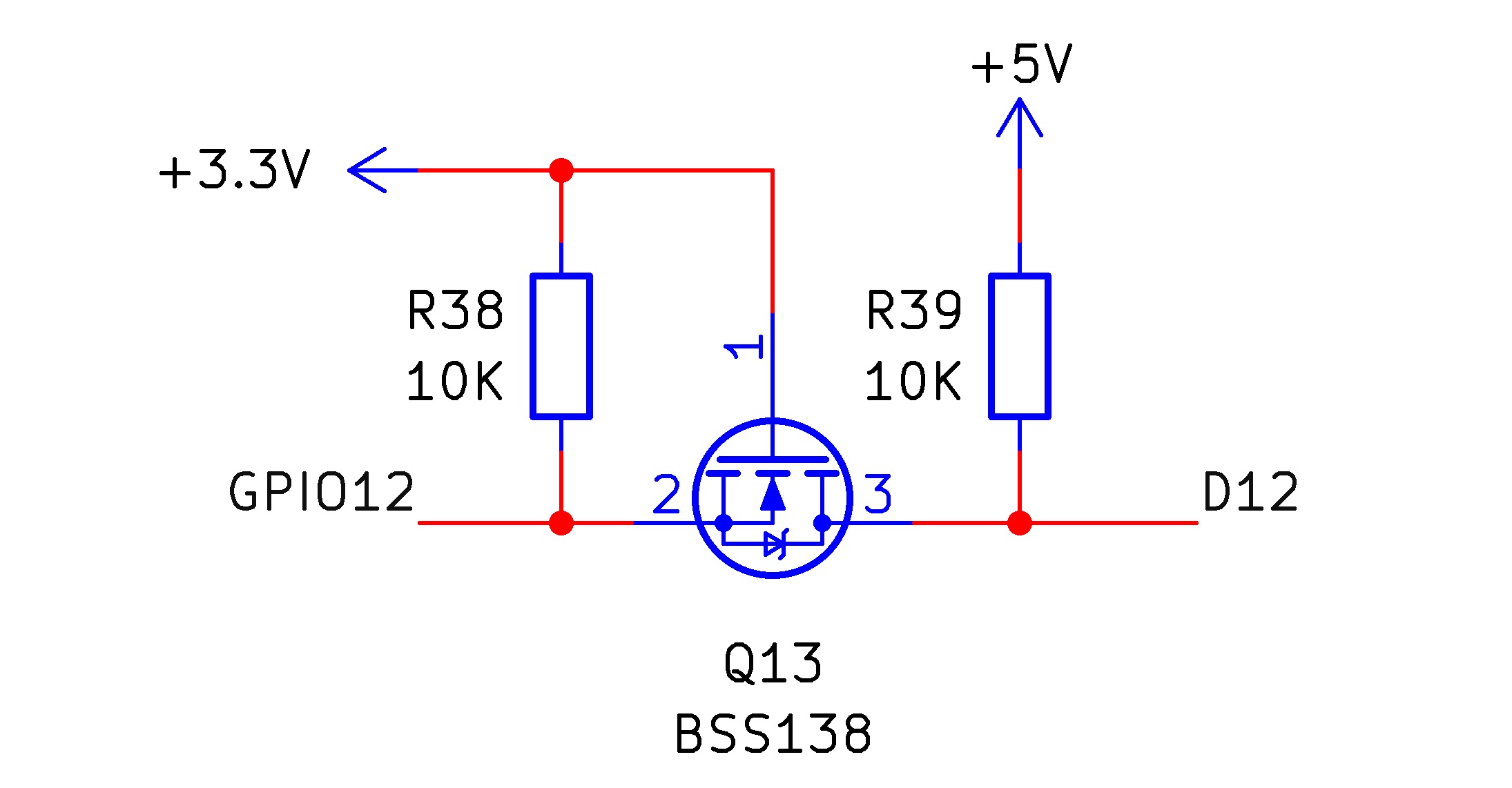
This circuit allows a signal to move between the two voltage domains without applying 5V directly to the RP2040 GPIO. It is especially well suited to open-drain signalling, where pull-up resistors define the logic-high voltage on each side.
The same translation also means the external pin should not be treated like a direct, high-current GPIO output. Pull-up values, connected capacitance and the type of interface all affect rise time and practical switching speed.
The translation circuitry is what gives RP-Duino its compatibility advantage, but it also becomes part of the electrical behaviour of every translated signal.
GPIO & analogue inputs
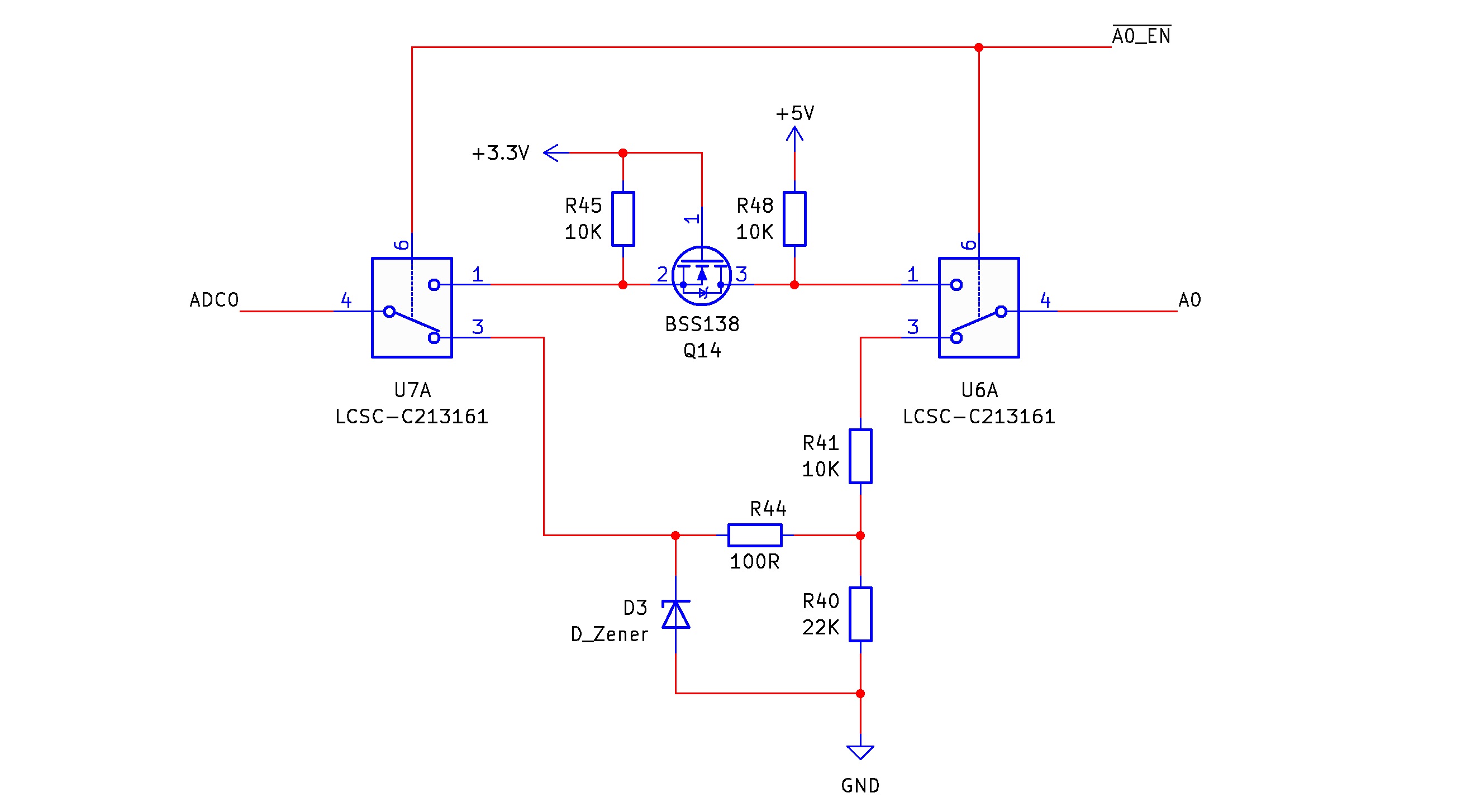
The Uno-style analogue header has to support both analogue measurement and digital I/O. RP-Duino handles this by providing separate analogue and translated-digital paths that can be selected in software.
Each analogue header pin can be routed towards the RP2040 ADC path or used as a translated digital I/O. The analogue-enable controls use GPIO22 through GPIO25 and are active low.
For example, to use A0 as an analogue input, configure GPIO22 as an output and drive it low. To use A0 as a digital I/O pin, drive the corresponding enable high so the digital path is selected instead.
Connects the conditioned analogue path to the RP2040 ADC.
Selects the translated digital I/O path for the header pin.
Board reference
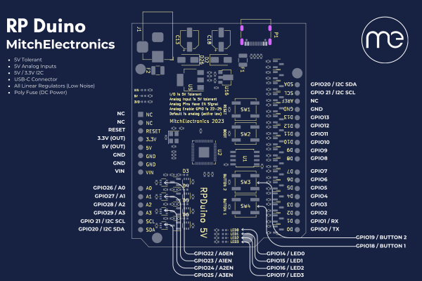
The original board pinout is retained here as a quick reference when wiring shields, modules or direct connections.
Engineering trade-offs
5V tolerance is useful precisely because extra circuitry sits between the microcontroller and the header. That circuitry solves one problem while introducing limits that need to be understood in more demanding designs.
The pull-up resistors and connected capacitance influence rise time. Lower resistance can improve switching speed, but it also increases current, so the interface is a deliberate compromise rather than an ideal logic buffer.
The translated channels already include pull-up behaviour. Circuits that depend on an unusual high-impedance or externally pulled configuration should be checked against the complete signal path.
The 5V-tolerant analogue path conditions the incoming voltage before it reaches the RP2040 ADC. Software should therefore use the board's actual scaling rather than assuming a direct 0–3.3V ADC connection.
RP-Duino is intended to make mixed-voltage development and migration from 5V hardware easier. For very high-speed buses, precision analogue measurement or unusual electrical loads, treat the level-shifting and analogue front end as part of the design and verify the interface accordingly.
RP2040 without abandoning 5V hardware
Use the familiar Uno format, modern RP2040 processing and board-level voltage translation to bring older hardware into newer projects.