
Interactive electronics resource
Logic Probe Kit Instructions
Build, understand and experiment with the Logic Probe Kit. This resource brings the original kit material into the current MitchElectronics format with the schematic, circuit explanation, component and PCB information, construction guidance, troubleshooting and practical ideas where available.
Introduction
The problem with multimeters
Testing circuits can be done with multi-meters and oscilloscopes but this is not always the best method. For example not everyone has access to an oscilloscope and multi-meters are no good for fast changing signals. Another reason is ease of use, testing a circuit with an oscilloscope can be tricky as you need to probe the contact and then turn away to look at the display. All it takes is for the probe to slip slightly and then the oscilloscope will be showing the signal trace for a completely different connection.
Meet the logic probe!
This is where the faithful logic probe saves the day! Instead of having numbers to show voltages or a display to show signals over time the logic probe has just three LEDs for outputs. These outputs can show the following conditions:
- Red Only - Logic 0
- Yellow Only - Floating
- Green Only - Logic 1
- All LEDs - Oscillating
So long as the probe has a common ground to the circuit under test (which can be done easily by either using the same power supply or connecting the The logic probe in all its glory probes GND-REF to the ground of the circuit), the probe will display one of the four listed conditions above when the probe contact is connected to a point in the circuit. But how does this probe work? Read on and find out!
Schematic
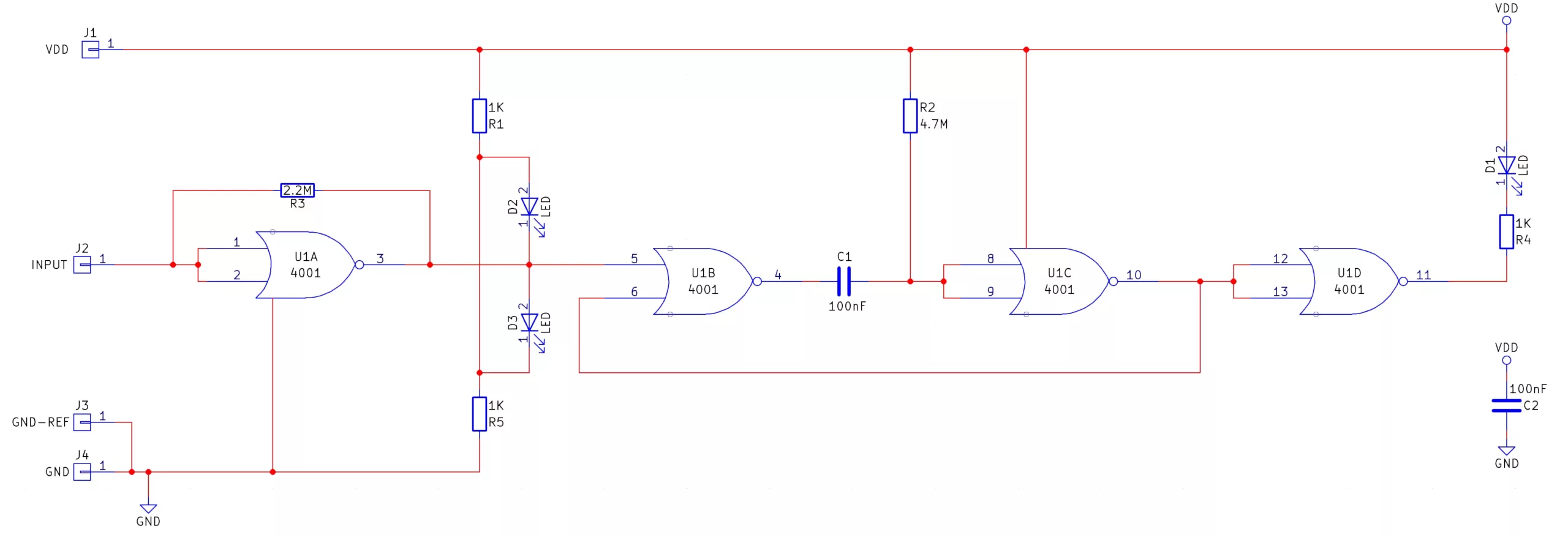
How does the logIC probe work?
The logic probe uses a 4001 quad NOR gate IC, resistors and a capacitor. The first NOR gate is used as a basic oscillator. With the inputs connected together the first NOR gate is transformed into an inverter. R3 is used to feed the output back into the input which results in oscillation if the input is unconnected (floating).
D2 is connected between power through R1 and the output of the NOR gate while D3 is connected to ground through R5 and the output of the NOR gate. If the input to the NOR gate is a logical 1 then the NOR gate will output 0V and this will result in D2 turning on (current flows through R1, through D2 and then into the output which is at 0V). If the input is off then the output of the NOR gate will be VDD and this results in D3 turning on instead of D2 (current flows from the output of the NOR gate through D3 and then to ground through R5).
The next two NOR gates form a basic mono-stable circuit which is used to detect an oscillating signal. If for example, the input signal was oscillating at a high rate (more than a MHz), then any LED that is used to show this signal would not be very bright and thus make it hard to tell if the input is oscillating. To solve this the mono-stable formed by the second two NOR gates, capacitor (C1) and resistor (R2) will be constantly triggered and re-triggered by the oscillating input. This results in a constant output which will make an LED bright so long as the oscillation is present. The last NOR gate is used as an LED driver for the mono-stable.
If no input is connected (floating), the NOR gate will weakly oscillate around VCC / 2. The voltage seen by both D2 and D3 will be approximately half VCC and thus results in neither LED turning on and therefore indicates a floating input. This weak oscillation, however, is able to set and reset the monostable which keeps the yellow LED on.
Note on using the logIC probe!
The logic probe will only work properly if the GND-REF pad is connected to the ground of the circuit under test. If the ground in the logic probe is not the same as that of the test circuit then there is no return path for any signals which results in the logic probe not being able to take measurements.
In other words, signals can only be measured with respect to some level. There is no such thing as an absolute voltage, voltage is relative because it is always with respect to some user-defined point. A common example is the mains wiring: The neutral wire is 230VAC with respect to the live wire but 0VAC with respect to earth (and hence you).
Try it yourself
Circuit simulation
Not available in mobile view
What you need
Component List
| Component | Quantity | PCB Reference |
|---|---|---|
| 14 DIP Socket | 1 | U1 |
| 4001 | 1 | U1 |
| 100nF Capacitor | 2 | C1, C2 |
| 1K Resistors | 3 | R1, R4, R5 |
| 2M2 Resistor | 1 | R3 |
| 4M7 Resistor | 1 | R2 |
| Green LED | 1 | D2 |
| Yellow LED | 1 | D1 |
| Red LED | 1 | D3 |
| Pogo Pin | 1 | J2 |
| Red Wire | 1 | VDD |
| Black Wire | 2 | GND, GND-REF |
| Logic Probe PCB | 1 | — |
Inspect the board
Interactive BOM
Board reference
PCB & assembly
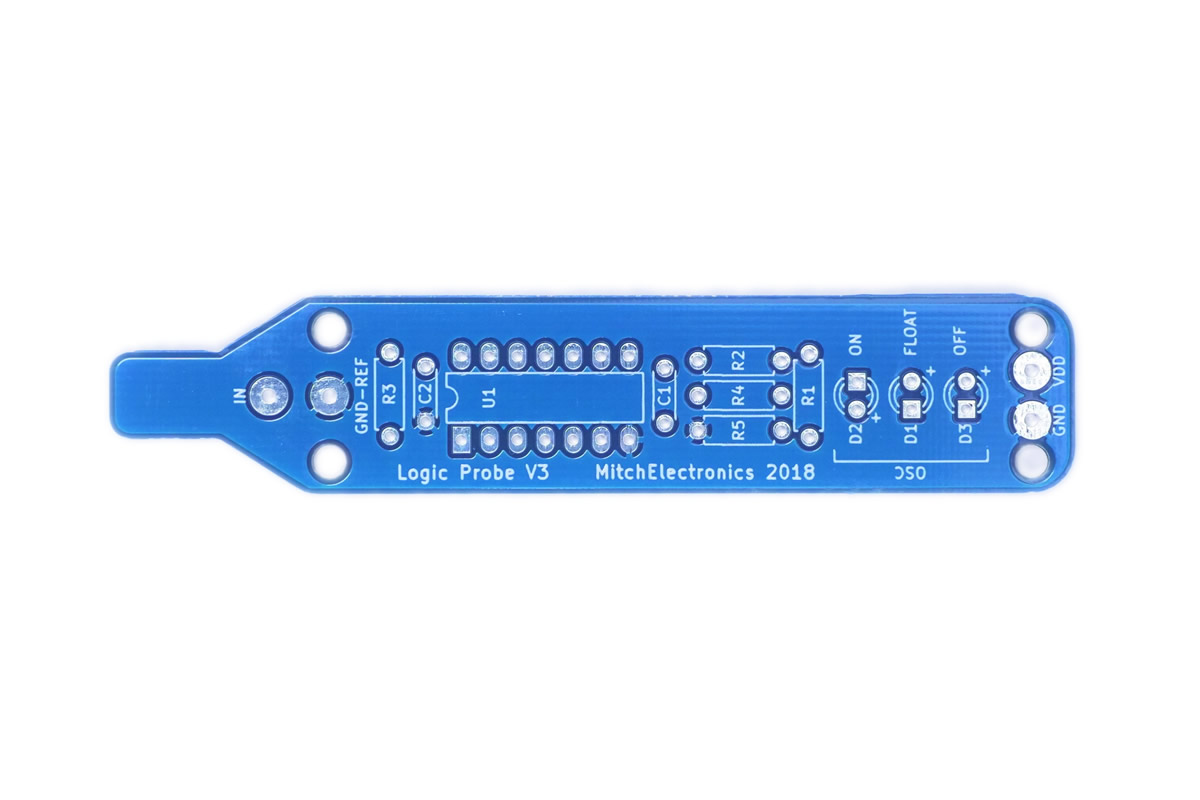
The PCB silkscreen and component references should be checked against the component list before soldering each part.
Before applying power
- Check every component against its PCB reference.
- Confirm the orientation of all polarised components and ICs.
- Inspect for solder bridges, unsoldered pads and clipped leads that could cause a short.
- Check that no loose wire or solder debris remains on the board.
Build with confidence
Construction tips
Recommended build order
A reliable way to assemble Logic Probe Kit is to work from the lowest-profile components to the tallest. This keeps the PCB easy to access while you solder.
- Fit resistors, links and other low-profile components first.
- Fit small capacitors and diodes, checking polarity where applicable.
- Fit IC sockets and small semiconductors, observing the orientation markings.
- Fit larger capacitors, potentiometers, switches and other controls.
- Fit LEDs, connectors and the remaining taller components.
- Insert socketed ICs only after soldering around the socket is complete.
- Inspect every joint and check for solder bridges before applying power.
Electronics construction guidance
If you are new to kit construction, use the Soldering Guide alongside these instructions. Identify each component before fitting it and compare its reference with the component list and PCB silkscreen.
When it does not work
Troubleshooting
Nothing happens when power is applied
- Confirm the supply is connected to the correct input and with the correct polarity.
- Check that ICs, diodes, LEDs, transistors and electrolytic capacitors are fitted in the correct orientation.
- Compare component values and positions against the component list and PCB reference.
- Inspect for missed joints, dry joints and accidental solder bridges.
The circuit powers up but does not behave as expected
This kit is intended for digital logic-level probe. If the output is stuck, unstable or outside the expected behaviour, use the schematic to trace the circuit a stage at a time rather than replacing several parts at once.
Check the components around the part of the circuit responsible for the output or timing first. A misplaced resistor, reversed semiconductor or poor connection can allow a circuit to power up while preventing it from operating correctly.
The circuit works intermittently
Intermittent behaviour is often caused by a marginal solder joint, a loose connector or a component lead that has not been fully soldered. Gently inspect the board with power removed and reflow any joint that looks dull, cracked or incomplete.
If the fault remains, compare the assembled board with the schematic and PCB reference one connection at a time.
Ready to test and experiment?
Did you know you can combine multiple logic probes into a singular unit to allow for multiple logic tests Click here to find out how to build this project...
Once the board is working, compare its behaviour with the schematic and the explanation above. Try changing only one input, control or permitted component value at a time so you can clearly see what effect that change has on the circuit.