Prepare the bench
- Soldering iron and stand
- Wet sponge or tip cleaner
- Lead-free solder
- Small pliers and wire cutters
- Screwdrivers and tweezers

Interactive electronics resource
A practical guide to identifying, fitting and soldering the common components used in MitchElectronics kits.
01 / Getting started
Good construction starts before the soldering iron is switched on. Identify the parts, PCB references and tools you need first.
0 of 5 checks complete
Fit low-profile components such as resistors first. Larger controls, buzzers and connectors are normally easier to add later.
02 / Core skill
A good joint is made by heating the PCB pad and component lead together, then allowing solder to flow across the connection.
03 / Assembly order
Working from the physically smallest parts to the tallest keeps the PCB accessible and makes it easier to hold components in place.
Select a stage to jump to the relevant component guidance.
04 / Component guide
Search by component name or PCB reference. Open only the sections you need for the kit in front of you.
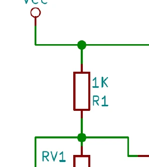
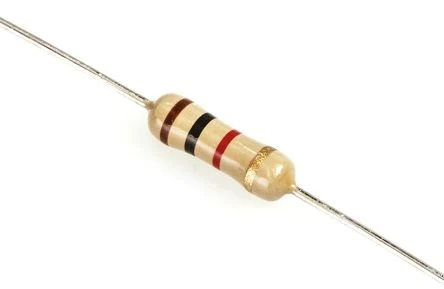
Resistors are normally fitted early because they sit close to the PCB and are among the smallest through-hole components. The schematic and PCB use the same R-number.
The resistor value tells you what to fit; the R-number tells you where to fit it.

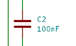
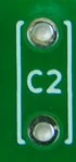
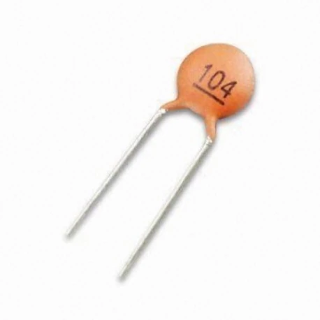
Match the C-number to the PCB. Ceramic capacitors in this guide are non-polarised. Fit them a few millimetres above the PCB, solder both leads and trim the excess.
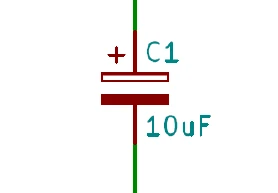
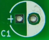
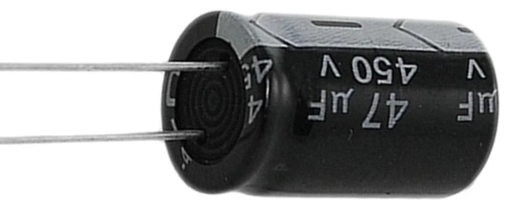
Electrolytic capacitors are polarised. The positive lead is normally longer, while the negative side is marked by a stripe on the body.
The PCB example uses a square pad for positive. Confirm both the component and PCB marking before making the joint.
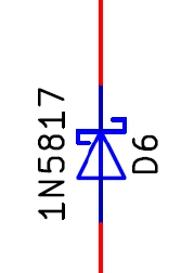
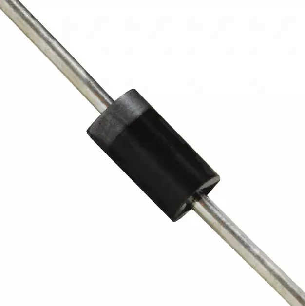
The band on a diode marks the cathode side. Match the band to the cathode indication on the PCB outline.

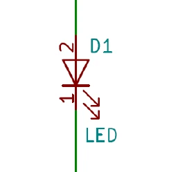
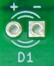
The longer lead is the anode and the shorter lead is the cathode. Do not trim the leads until the LED has been fitted and soldered.
In the source board shown here, the square pad is the cathode and the round pad is the anode.

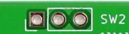
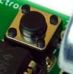
Switches are commonly identified with S or SW followed by a number. Tactile switches have formed legs that click into the PCB when fully inserted, helping them sit flat before soldering.
The retaining-leg click is a useful sign that a tactile switch is fully inserted.
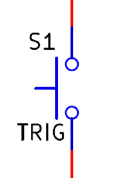
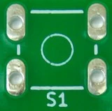
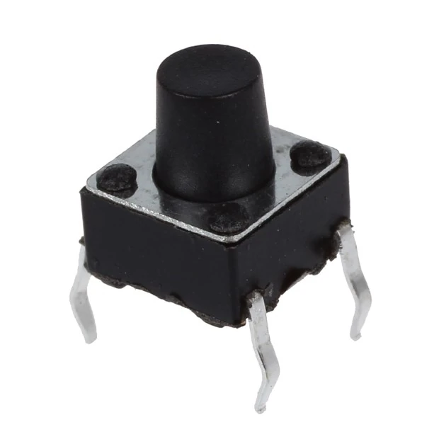
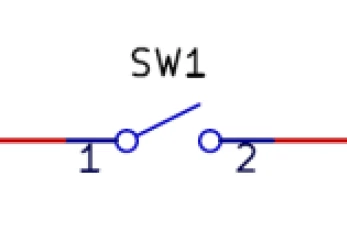
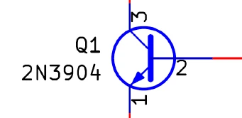
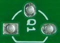
Transistors are identified with Q followed by a number. The kits described in the source guide commonly use TO-92 devices. Match the curved and flat sides of the package to the PCB outline.
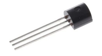
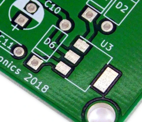
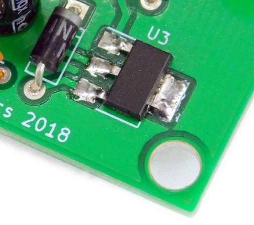
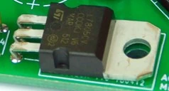
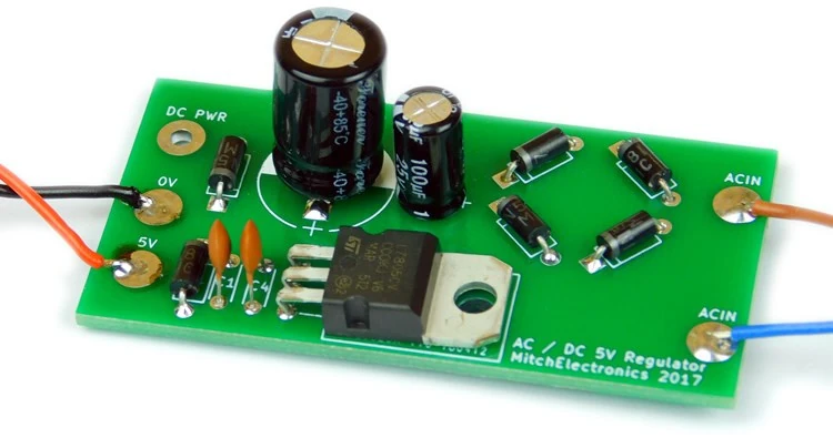
Regulators are integrated circuits and use U or IC references. TO-92 parts are fitted much like transistors. TO-220 packages are larger and easier to hold while soldering.
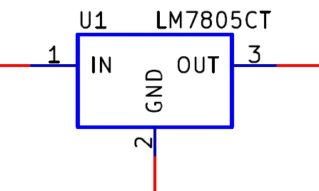
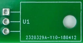
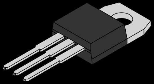
For the AMS1117-style example, tin the large tab pad first. Hold the device in position with tweezers while reheating that pad, then solder the three smaller leads once it is secured.
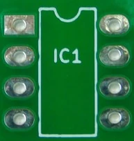
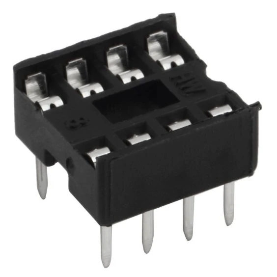
IC sockets allow the socket to be soldered first and the IC to be inserted only after the rest of the circuit has been assembled.
PCB outline, socket and IC should all indicate the same orientation.
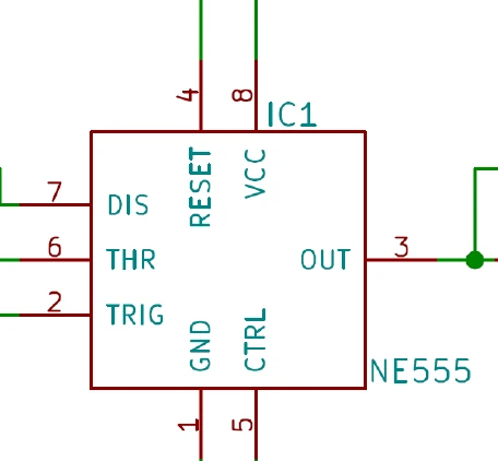
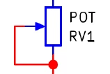
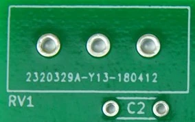
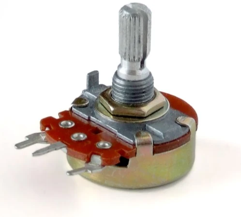
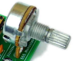
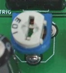
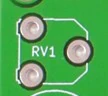
Potentiometers are identified by RV followed by a number. Larger types are usually fitted later. Their orientation matters mainly because the shaft or adjustment point must remain accessible.
Insert the part, turn the PCB over and let the board rest on the component while soldering. Small trim potentiometers usually fit in only one physical orientation.
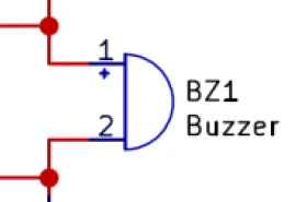
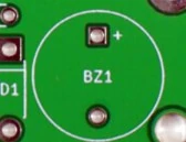
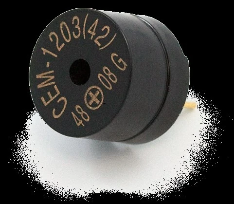
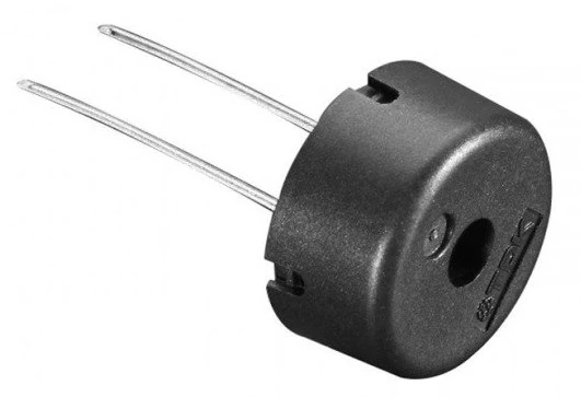
Buzzers are typically identified by BZ. For a polarised buzzer, the positive connection can be identified by the longer lead or a plus mark on the body.
Some buzzers are not polarised and may have equal-length pins. Check the kit instructions when the part is not marked.
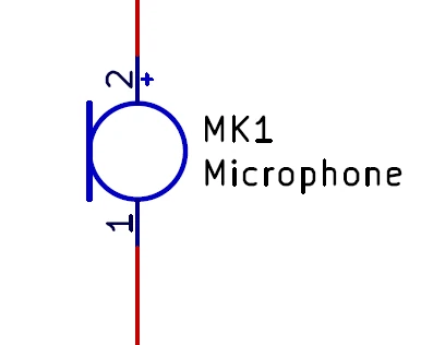
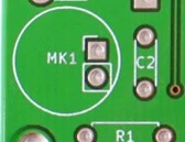
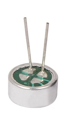
The electret microphones shown in the source guide are polarised. Their leads may be equal length, so polarity is identified from the underside.
The lead connected by small traces to the metal case is the negative connection. The other lead is positive. In the PCB example, positive is fitted to the square pad.
Lead length is not a reliable polarity cue for these microphones.

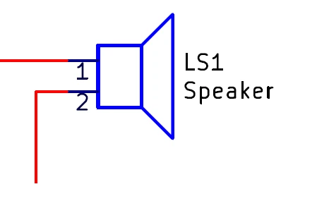
Speakers are marked with positive and negative terminals. Polarity is most important when multiple speakers need to move in phase; for a simple single-speaker kit it is generally less critical.
Do not solder to the delicate contacts carrying the tiny wires into the speaker coil. Use the intended external solder pads.
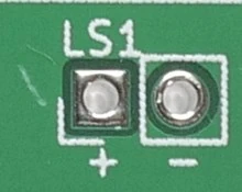
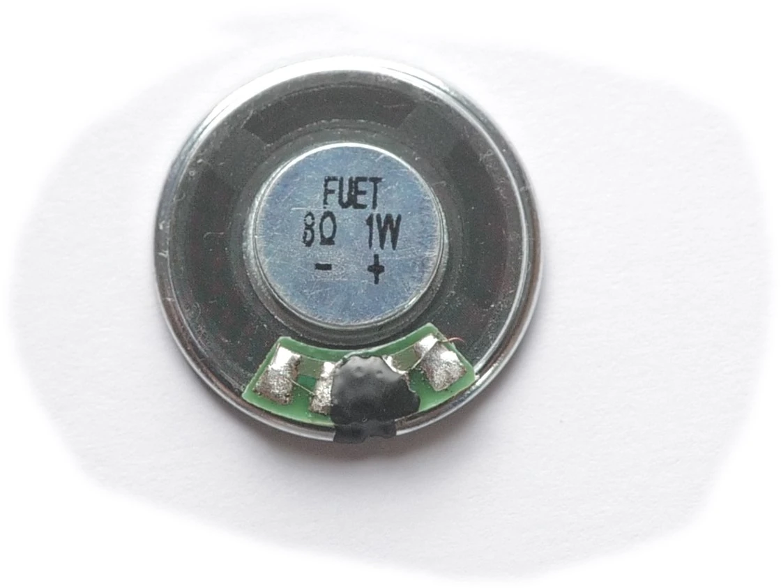
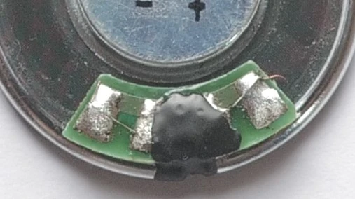
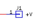
Wires connect the finished circuit to power, inputs and outputs. Connection points are often marked with P or J references.
Recommended for positive supply connections such as VDD and VCC.
Recommended for GND, VSS and 0 V connections.
Consistent power wiring makes the final assembly easier to inspect and reduces ambiguity.

Try a name such as LED, capacitor, or a reference such as Q or RV.
05 / Before power
A few deliberate checks before applying power can catch most assembly mistakes without any fault-finding.
Use this guide whenever you need to confirm a reference, orientation or fitting method.
Keep learning
Return to the resource library for kit instructions, circuit explanations, calculators and other practical electronics guides.