
Interactive electronics resource
Discrete Op-Amp Kit Instructions
Build, understand and experiment with the Discrete Op-Amp Kit. This resource brings the original kit material into the current MitchElectronics format with the schematic, circuit explanation, component and PCB information, construction guidance, troubleshooting and practical ideas where available.
Introduction
Basics of Op-Amps
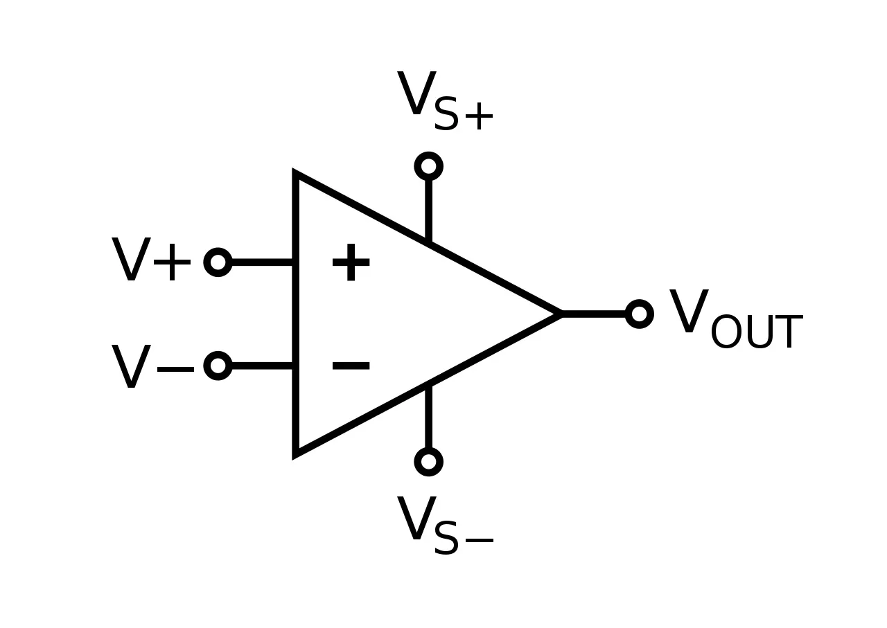
Even if you are new to electronics, you most likely have used an op-amp. If not, an op-amp stands for operational amplifier and has the symbol shown on the right. The op-amp has two inputs (+ and -), two power pins and single output. While the maths behind op- amp circuits can be complex the basic formula that shows the output voltage is given as:
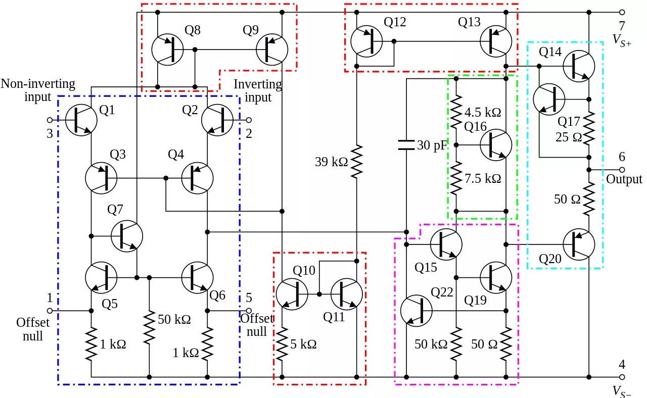
By using a combination of other components the op-amp can be used to make many different circuits ranging from amplifiers to oscillators. But op-amps that you typically use in a circuit are in a small plastic package and to most are considered black boxes (something that just works). An example of a famous op-amp, the 741, is shown on the right with its schematic.
But this kit will not only let you build your own basic op-amp but will also teach you the basics of how they actually work!
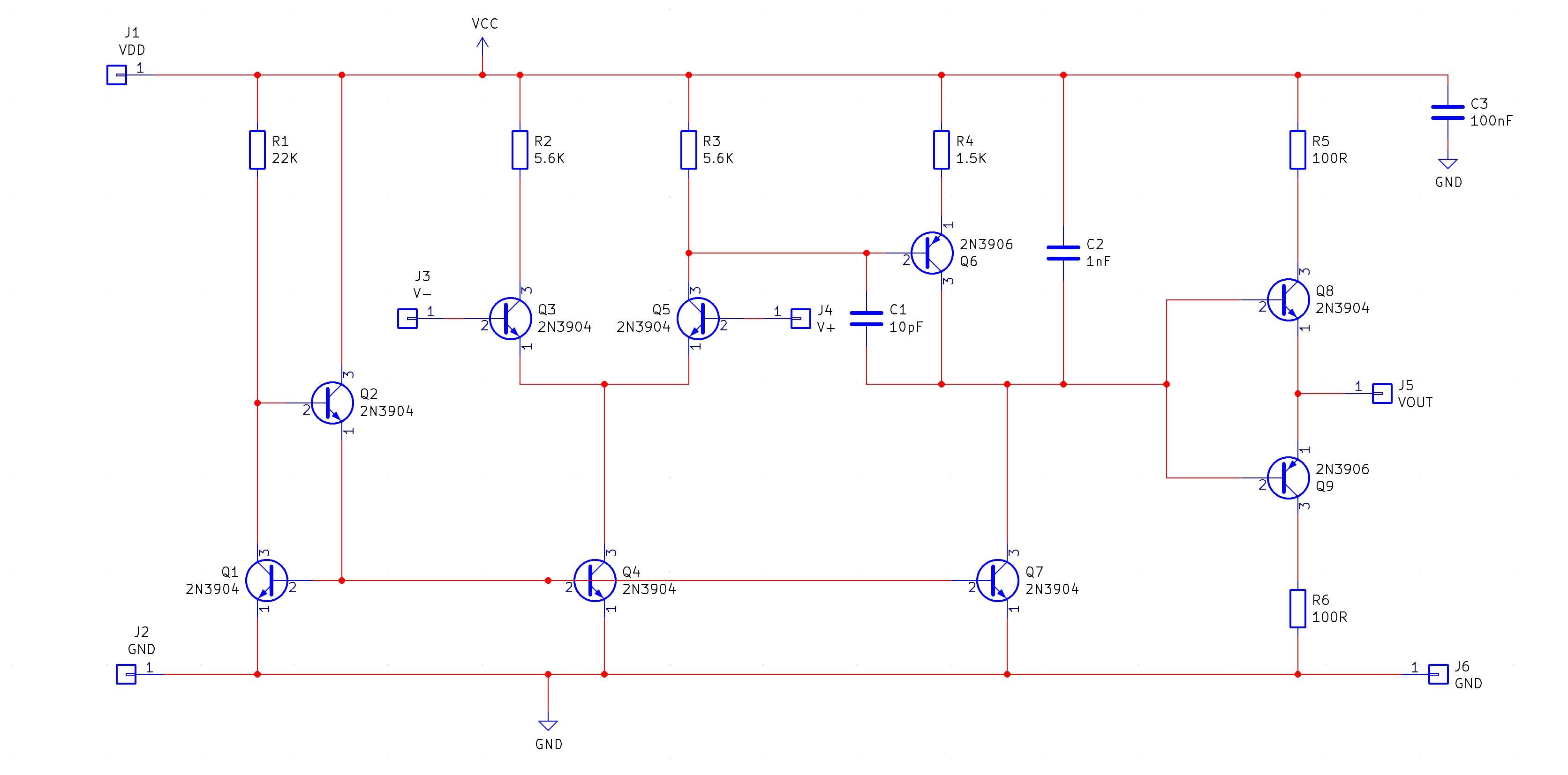
Schematic
How does the discrete Op-Amp work?
The Main Components
The op-amp consists of several stages:
- Q3, Q4 and Q5 form the input stage
- Q1 and Q2 form a constant current source (keeps Q4 and Q7 current constant)
- Q6 forms an amplifier to increase the open loop gain of the op amp
- Q8 and Q9 consist of a push-pull amplifier which is the output stage
Input Stage
If both input voltages are the same both Q3 and Q5 will conduct the same current. If the V+ input (Q5) increases then Q5 will be able to conduct more current and as a result does. So now that more current is flowing through Q5 means that the current flowing through Q3 needs to reduce. This is because Q4 can only conduct a limited amount of current (controlled by the current mirror Q1 and Q2), and so if more current flows through Q5 then less current flows through Q3 which leaves the current in Q4 un- changed. Since the effective resistance of Q5 has been reduced (as it is now conducting more), the voltage at the collector of Q5 decreases.
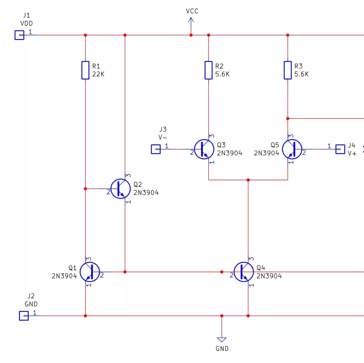
If the voltage on V- (Q3), increases then the same will happen as before except the current through Q3 will increase and the current through Q5 will decrease since the total current that can be conducted is limited by Q4. Since Q5 now conducts less its effective resistance has increased and thus the voltage at the collector of Q5 increases.
Amplification Stage
The output of the input stage (Q5 collector), is fed into a PNP transistor (Q6), which has an NPN transistor (Q7), acting as a resistor. If the input voltage to this stage increases then the output of the amplifier (Q6 collector), will decrease. This is because an increase in the input voltage makes the base-emitter region of the PNP transistor more positive which results in the PNP transistor conducting less. When Q6 conducts less the voltage drop across the active load (Q7), will therefore also drop.
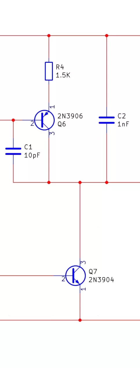
If the output from the input stage decreases then the base-emitter voltage of Q6 will become more negative (as the emitter is at a larger positive voltage than the base), and thus Q6 will conduct more. The current through the active load will therefore increase and result in a larger voltage drop across Q7. C1 is a very special capacitor which stops oscillations. It has a very specific name, a miller capacitor. The miller effect is complex to understand but simply put the capacitor ensures that the gain of the op-amp falls below 1 before the phase shift reaches 180 degrees.
Output Stage
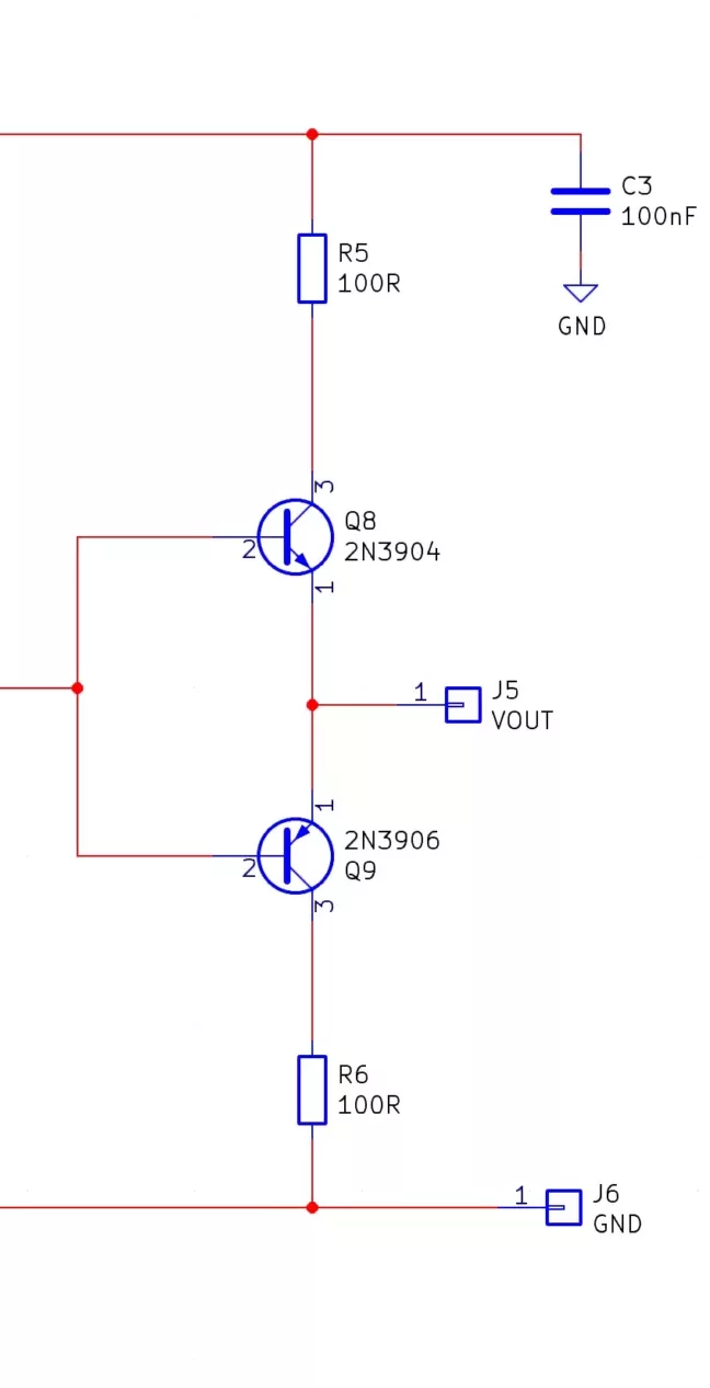
The output stage consists of a push pull amplifier (Q8 and Q9), with current limiting resistors (R5 and R6). The input to the output stage is connected to the output of the amplifier stage. Simply put, if the input to the output stage increases then the output voltage will increase. If the input voltage decreases then the output voltage will be lower.
Summary
So now that we have looked at each part let’s run through the whole design again briefly to fully understand the nature of op-amps!
An increase in V+
- Q5 conducts more and thus Q3 conducts less
- Voltage across Q5 collector therefore reduces
- Amplifier stage is inverting and a reduction in the input results in a larger output
- This increase in output voltage is passed to the push-pull amplifier
- The output voltage increases
An increase in V-
- Q3 conducts more and thus Q5 conducts less
- Voltage across Q5 collector therefore increases
- Amplifier stage is inverting and an increase in the input results in a smaller output
- This decrease in output voltage is passed to the push-pull amplifier
- The output voltage decreases
Project ideas
Basic Audio Amplifier
The Discrete Op-Amp kit has terrible characteristics for an amplifier which is why it is an excellent teaching tool. However, it can still be used as a practical amplifier which is why using it in other projects can provide great insight into amplifier selection.
One such experiment would be to use the Discrete Op-Amp as an audio amp. Connecting the Discrete Op-Amp to a small signal source, amplify by configuring the Discrete Op-Amp as a non-inverting amplifier, and then connect the output to a speaker input. Does it work? What challenges did you face?

Clock Source
Interestingly, op-amps can be used as square wave oscillators if used in an inverting Schmitt trigger configuration with an RC circuit. This can be used to create synthesisers as well as provide a clock signal for microprocessing systems and digital circuits.
Alarm Circuit
Even though the Discrete Op-Amp may have poor characteristics, it doesn’t mean it can’t be used in other circuits. For example, the Discrete Op-Amp could be used as a comparator in an alarm circuit. By comparing the output voltage of a sensor to a potentiometer, it’s possible for the Discrete Op-Amp to produce a signal upon detecting a change in the output of a sensor. How reliable is such a system? Could you defend your house against intruders with such an amplifier?

Try it yourself
Circuit simulation
Not available in mobile view
What you need
Component List
| Component | Quantity | PCB Reference |
|---|---|---|
| 2N3904 | 7 | Q1, Q2, Q3, Q4, Q5, Q7, Q8 |
| 2N3904 | 2 | Q6, Q9 |
| 10pF Capacitor | 1 | C1 |
| 1nF Capacitor | 1 | C2 |
| 100nF Capacitors | 1 | C3 |
| 100R Resistors | 2 | R5, R6 |
| 1.5K Resistor | 1 | R4 |
| 5K6 Resistor | 2 | R2, R3 |
| 22K Resistor | 1 | R1 |
| Red Wire | 1 | VDD |
| Green Wire | 2 | V+, VOUT |
| Blue Wire | 1 | V- |
| Black Wire | 2 | GND |
| Discrete Op-Amp PCB | 1 | — |
Inspect the board
Interactive BOM
Board reference
PCB & assembly
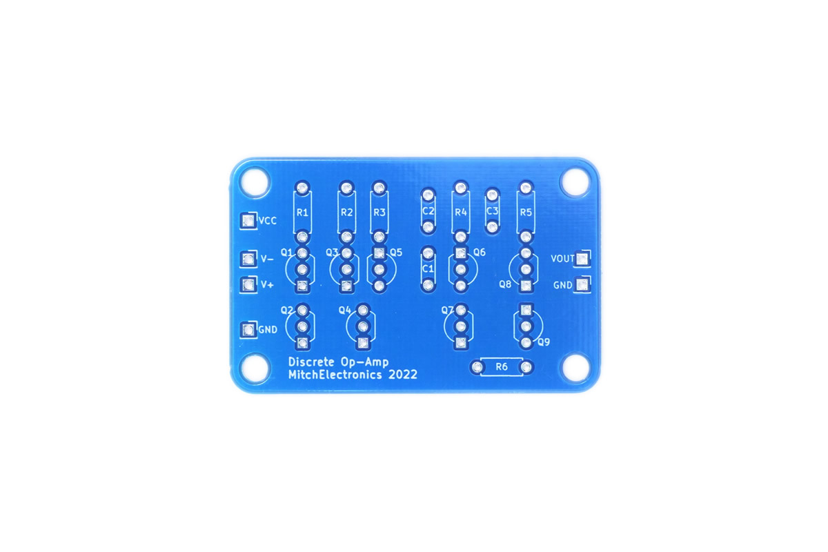
The PCB silkscreen and component references should be checked against the component list before soldering each part.
Before applying power
- Check every component against its PCB reference.
- Confirm the orientation of all polarised components and ICs.
- Inspect for solder bridges, unsoldered pads and clipped leads that could cause a short.
- Check that no loose wire or solder debris remains on the board.
Build with confidence
Construction tips
Recommended build order
A reliable way to assemble Discrete Op-Amp Kit is to work from the lowest-profile components to the tallest. This keeps the PCB easy to access while you solder.
- Fit resistors, links and other low-profile components first.
- Fit small capacitors and diodes, checking polarity where applicable.
- Fit IC sockets and small semiconductors, observing the orientation markings.
- Fit larger capacitors, potentiometers, switches and other controls.
- Fit LEDs, connectors and the remaining taller components.
- Insert socketed ICs only after soldering around the socket is complete.
- Inspect every joint and check for solder bridges before applying power.
Electronics construction guidance
If you are new to kit construction, use the Soldering Guide alongside these instructions. Identify each component before fitting it and compare its reference with the component list and PCB silkscreen.
When it does not work
Troubleshooting
Nothing happens when power is applied
- Confirm the supply is connected to the correct input and with the correct polarity.
- Check that ICs, diodes, LEDs, transistors and electrolytic capacitors are fitted in the correct orientation.
- Compare component values and positions against the component list and PCB reference.
- Inspect for missed joints, dry joints and accidental solder bridges.
The circuit powers up but does not behave as expected
This kit is intended for discrete operational-amplifier learning circuit. If the output is stuck, unstable or outside the expected behaviour, use the schematic to trace the circuit a stage at a time rather than replacing several parts at once.
Check the components around the part of the circuit responsible for the output or timing first. A misplaced resistor, reversed semiconductor or poor connection can allow a circuit to power up while preventing it from operating correctly.
The circuit works intermittently
Intermittent behaviour is often caused by a marginal solder joint, a loose connector or a component lead that has not been fully soldered. Gently inspect the board with power removed and reflow any joint that looks dull, cracked or incomplete.
If the fault remains, compare the assembled board with the schematic and PCB reference one connection at a time.
Ready to test and experiment?
Connect V- to the output pin and slowly increase the input voltage Create an inverting and non-inverting amplifier using resistors Try creating a simple RC oscillator
Once the board is working, compare its behaviour with the schematic and the explanation above. Try changing only one input, control or permitted component value at a time so you can clearly see what effect that change has on the circuit.