
Interactive electronics resource
Continuity Probe Kit Instructions
Build, understand and experiment with the Continuity Probe Kit. This resource brings the original kit material into the current MitchElectronics format with the schematic, circuit explanation, component and PCB information, construction guidance, troubleshooting and practical ideas where available.
Introduction
The Continuity Probe is a DIY tool used to test the electrical continuity of a wire between two points (hence the name Continuity Probe). If two points have electrical continuity, the Continuity Probe beeps its on-board buzzer, and this helps to quickly determine continuity without needing to read a display. However, what makes this kit special is that it uses a tiny amount of external current with diode protection to prevent damaging external circuits (simply using a battery and a buzzer on its own is a quick way to damage sensitive devices).
The low external voltage is too small to damage anything, and the series limiting resistors prevent damage during a short circuit. To make probing easier, this kit uses pogo-pins which are spring-loaded contacts. Thus, a small amount of pushing force can be provided to ensure proper contact while reducing the risk of mechanical damage to either the probe or the circuit being tested.
Schematic
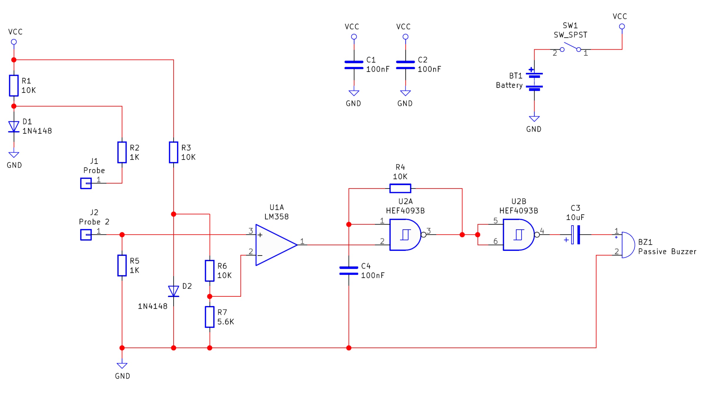
SCHEMATIC (Block diagram)
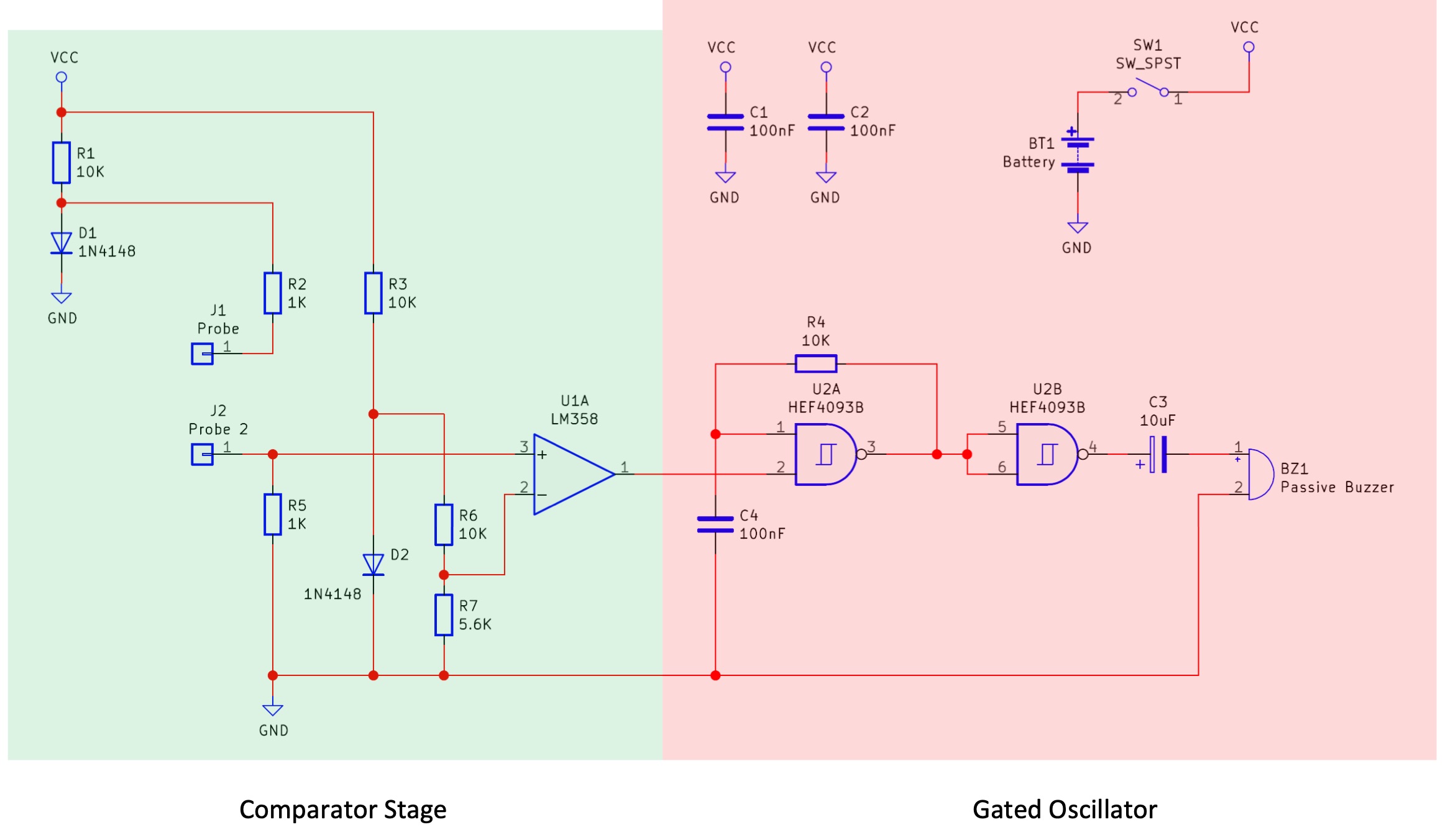
How does the continuity probe work?
No electronics workshop would be complete without a continuity probe but what exactly do they do? A continuity probe has two probe points that are used to determine if there is an electrical connection between two points. If the two probes probe the same wire then the continuity probe makes a beep sound and if there is resistance between the probe points (or no connection at all), then the continuity probe makes no sound at all.
A simple continuity probe could be built with a buzzer, a battery, and two probes which combine to make a simple buzzer circuit. While this is fine for checking the continuity of wires (ensure the wire is properly connected and undamaged), it is not recommended for potentially sensitive circuits. Applying power to a circuit can potentially cause reverse bias, or worse, a large current rush could damage components such as LEDs. Therefore, a proper continuity probe is needed to check for low resistance but not damage sensitive parts!
The MitchElectronics continuity probe is made up of two main sub-circuits
- Comparator circuit (U1)
- Gated Oscillator ( U2)
The comparator stage is made up of an op-amp and various components, whereby the two voltages that are compared are the voltage present at Probe 2, and the voltage across R7.
The voltage across R7 is approximately 0.6V * 1/3 = 0.2V, and if the two probes are not connected (i.e. there is no continuity), then the voltage across R5 is 0V which means that the output of op-amp U1A is 0V.
This output is fed into a gated RC oscillator made using a Schmitt trigger. If the input to the gated oscillator is 0V, then the output of the NAND gate stays high, and if the input is equal to VCC, then U2A can oscillate. This oscillation is buffered by the NAND gate U2B and this buffered square wave is fed into a buzzer.
When the two probes make electrical contact with each other (through a wire or PCB trace), the voltage across R5 is equal to 0.6V / 2 as the potential divider circuit (made up of R2 / R5) is connected to a forward-biased diode D1 whose forward voltage is 0.6V.
The 0.3V from this divider is greater than the 0.2V across the resistor R7, which means that the output of U1A goes to VCC when there is continuity between the two probes. The reason for using diodes to produce a 0.6V reference is to keep the voltages from the probes below 0.6V, which is low enough to prevent damage to sensitive parts such as ICs.
Try it yourself
Circuit simulation
Not available in mobile view
What you need
Component List
| Component | Quantity | PCB Reference |
|---|---|---|
| 8 DIP Socket | 1 | U1 |
| 14 DIP Socket | 1 | U2 |
| LM358 | 1 | U1 |
| 4093 | 1 | U2 |
| 100nF Capacitor | 3 | C1, C2, C4 |
| 10µF Capacitor | 1 | C3 |
| 1KΩ Resistor | 2 | R2, R5 |
| 5.6KΩ Resistor | 1 | R7 |
| 10KΩ Resistor | 4 | R1, R3, R4, R6 |
| 1N4148 Diode | 2 | D1, D2 |
| Buzzer | 1 | BZ1 |
| Switch | 1 | SW1 |
| Pogo Pin | 2 | PROBE 1, PROBE 2 |
| PP3 Connector | 1 | BT1 |
| Continuity Probe PCB | 1 | — |
Inspect the board
Interactive BOM
Board reference
PCB & assembly
The PCB silkscreen and component references should be checked against the component list before soldering each part.
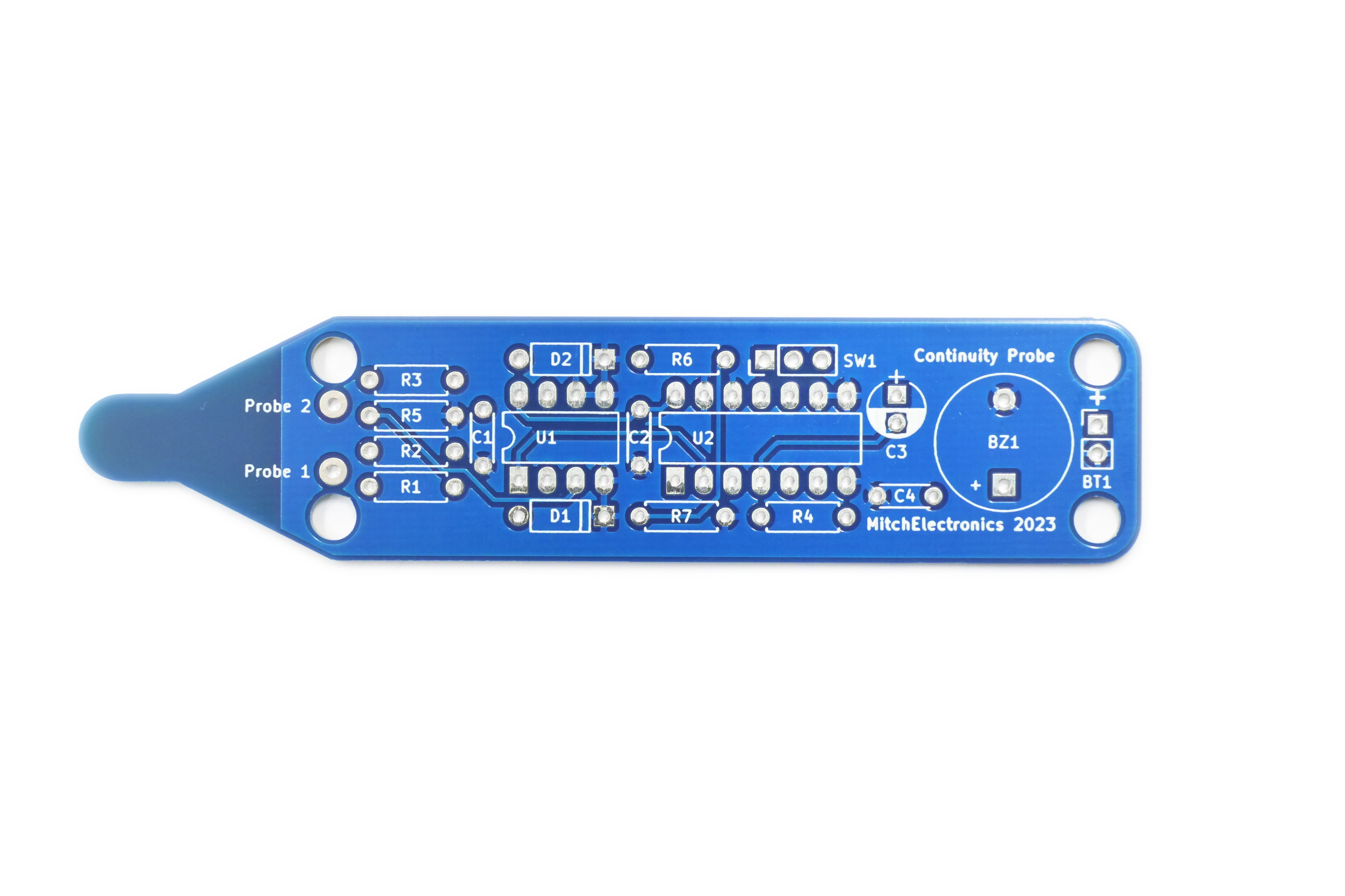
Before applying power
- Check every component against its PCB reference.
- Confirm the orientation of all polarised components and ICs.
- Inspect for solder bridges, unsoldered pads and clipped leads that could cause a short.
- Check that no loose wire or solder debris remains on the board.
Build with confidence
Construction tips
Recommended build order
A reliable way to assemble Continuity Probe Kit is to work from the lowest-profile components to the tallest. This keeps the PCB easy to access while you solder.
- Fit resistors, links and other low-profile components first.
- Fit small capacitors and diodes, checking polarity where applicable.
- Fit IC sockets and small semiconductors, observing the orientation markings.
- Fit larger capacitors, potentiometers, switches and other controls.
- Fit LEDs, connectors and the remaining taller components.
- Insert socketed ICs only after soldering around the socket is complete.
- Inspect every joint and check for solder bridges before applying power.
Electronics construction guidance
If you are new to kit construction, use the Soldering Guide alongside these instructions. Identify each component before fitting it and compare its reference with the component list and PCB silkscreen.
When it does not work
Troubleshooting
Nothing happens when power is applied
- Confirm the supply is connected to the correct input and with the correct polarity.
- Check that ICs, diodes, LEDs, transistors and electrolytic capacitors are fitted in the correct orientation.
- Compare component values and positions against the component list and PCB reference.
- Inspect for missed joints, dry joints and accidental solder bridges.
The circuit powers up but does not behave as expected
This kit is intended for electrical continuity tester. If the output is stuck, unstable or outside the expected behaviour, use the schematic to trace the circuit a stage at a time rather than replacing several parts at once.
Check the components around the part of the circuit responsible for the output or timing first. A misplaced resistor, reversed semiconductor or poor connection can allow a circuit to power up while preventing it from operating correctly.
The circuit works intermittently
Intermittent behaviour is often caused by a marginal solder joint, a loose connector or a component lead that has not been fully soldered. Gently inspect the board with power removed and reflow any joint that looks dull, cracked or incomplete.
If the fault remains, compare the assembled board with the schematic and PCB reference one connection at a time.
Ready to test and experiment?
Mounting this project inside of an enclosure can make it easier to use Consider using free software such as FreeCAD to design this Use a 3D printer to print the design
Once the board is working, compare its behaviour with the schematic and the explanation above. Try changing only one input, control or permitted component value at a time so you can clearly see what effect that change has on the circuit.