
Interactive electronics resource
4015 Shift Register Board Instructions
Build, understand and experiment with the 4015 Shift Register Board. This resource brings the original kit material into the current MitchElectronics format with the schematic, circuit explanation, component and PCB information, construction guidance, troubleshooting and practical ideas where available.
Introduction
Pre-learning – The Logic Gate Board
Before you learn how the 4013 D-Type Flip Flop Board works, you should first learn how the Logic Gate Board works as that kit covers the basics of logic. The Logic Gate Board kit also provides multiple logic chips in the 4000 series, demonstrating how these chips work and how some of the 4000 series share similar packages and configurations.
What is a shift register?
A shift register is a digital circuit that can both store and shift data, and shift registers are extremely important in modern logic devices (especially processors and peripherals).
In its simplest form, a shift register has a single data input, a clock input, and a parallel output showing all stored bits. When the clock input rises, all the data across the outputs is shifted once (with the very last output being thrown away), and the logic signal present on the input data pin is transferred to the very first output. Some shift registers also have a reset input which clears all the outputs.
This behaviour means that shift registers essentially convert a serial data signal (consisting of individual bits one at a time), into a parallel signal, and are commonly used in UART, SPI, and I2C peripherals.
What is the 4015 shift register?
As the name suggests, the 4015 is a shift register IC that belongs to the 4000 family of ICs. While the exact origin of this chip is not known, it is likely to have been developed around the late 1960s / early 70’s.
Using CMOS technology, the 4015 consumes virtually no power when unused, and very little power when in active operation (when the clock pin is being pulsed), making it ideal for battery and low-power applications. Furthermore, the 4015 is available in both through-hole DIP and surface mount SOIC packages, making it ideal for both breadboards and PCBs in mass production.
Inside the 4015 are two independent 4-bit shift registers, each having a data input, clock input, and reset. While these two shift registers work independently, they can be combined to create a larger 8-bit shift register if the last output of the first shift register is connected to the data input of the second shift register, and both clock and reset inputs connected together.
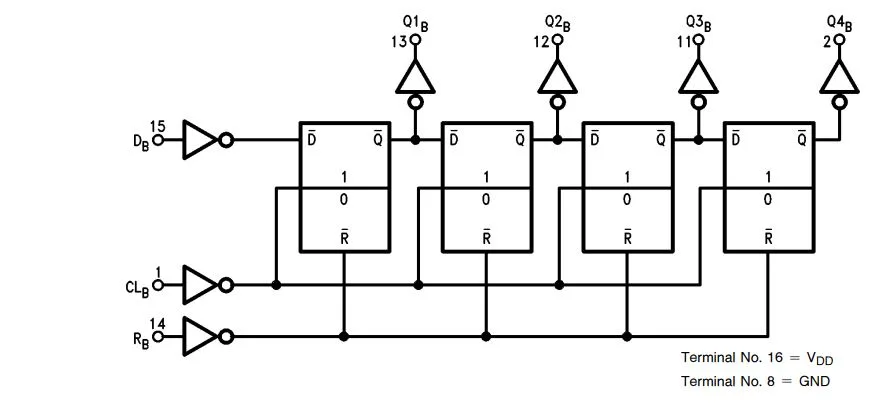
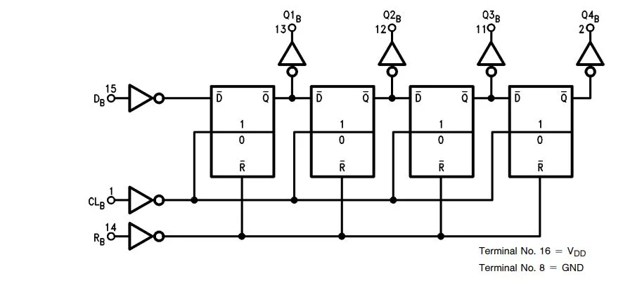
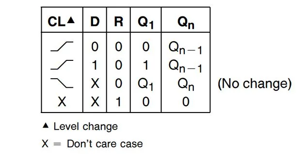
Schematic
How does the 4015 shift register board work?
The circuit
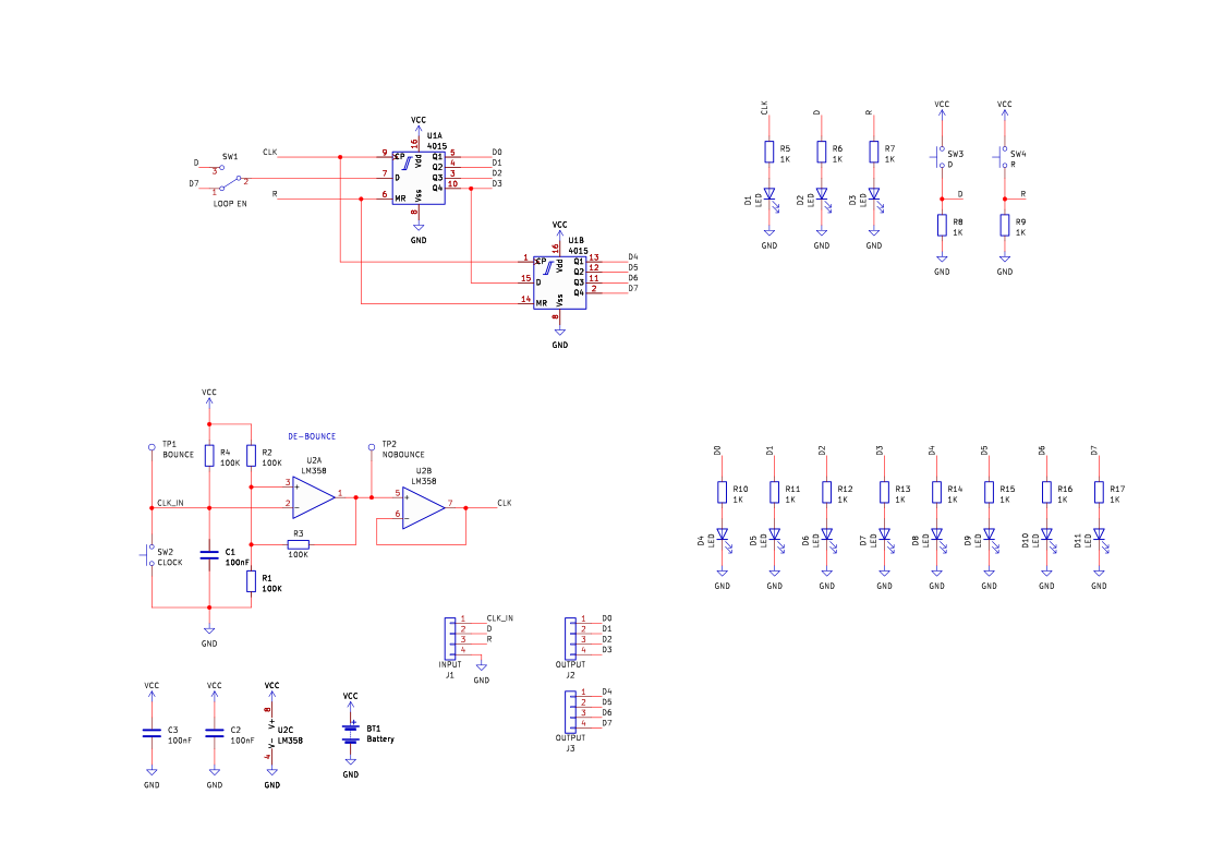
The Shift Register Board is a simple kit that lets you get soldering experience while also learning about the 4015 shift register. Instead of having two independent shift registers, the 4015 combines them into a single 8-bit shift register, thus demonstrating how shift registers can be chained together.
The board also integrates buttons for each control input, so that they can be independently tested, and each output of both shift registers has been connected to its own LED in a row, so you can see how data is shifted across. Furthermore, to prevent multiple clock pulses when pushing the clock button, a de-bounce circuit has been included, which ignores sudden multiple presses of the clock button.
Finally, all the input and outputs are passed through to two expander pads on the side of the PCB, allowing for future expansion with other logic boards.
Clock skew bug / Not a bug, but a feature!
When the 4015 kit was initially designed, it was assumed by our engineers that simply connecting the two independent shift registers together would be sufficient. However, while this is certainly the case in an ideal world, the real world that we actually live in is anything but.
Depending on environmental conditions, when using the shift register, it is possible for data from the first shift register to get shifted into the second shift register early, with data that arrives at the fourth LED also appearing on the fifth LED. The reason why this can happen comes down to the speed of electric signals.
In an ideal circuit, electricity arrives at its destination instantly, but in reality, electric pulses take time to move (propagate) through wires. For basic circuits like the 555 astable, transistor flasher, or discrete op-amp, this isn’t an issue as their state isn’t governed by nanosecond timing, but for logic circuits, this timing can be everything.
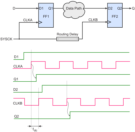
In the case of the 4015 kit, even though both shift registers use the same clock signal, it takes time for the signal to reach both shift registers (with the first shift register getting its signal first). Furthermore, it also takes time for the clock input to register a signal and activate the internal logic of the chip.
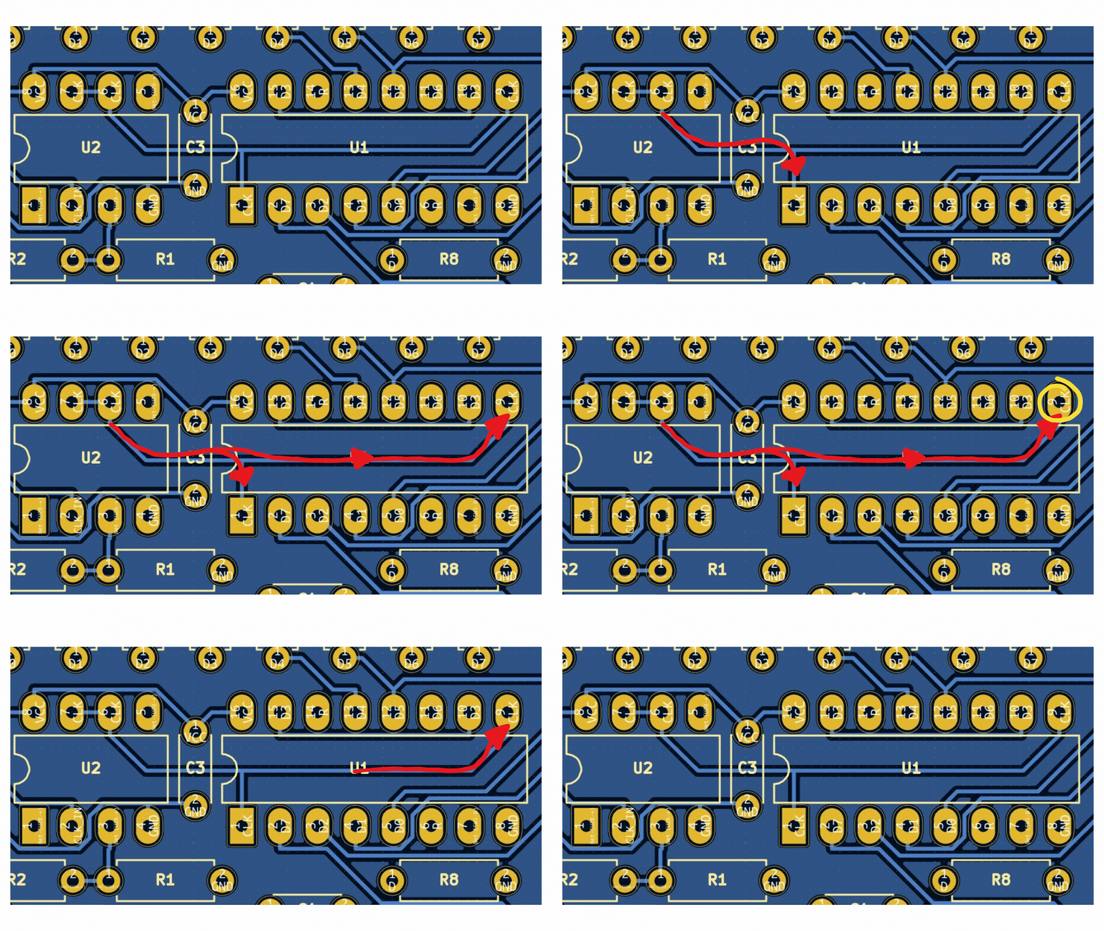
Thus, if the first shift register activates before the second shift register, it is possible for the last output of the shift register to also be passed onto the second shift register. This type of glitch is often called clock skew, and can cause major havoc in large digital circuits, such as CPUs.
How to fix clock skew
To fix clock skew, the best solution is to introduce a delay in the clock signal. One such method for introducing a delay is to include RC circuits which take time to charge (something which is used in the Discrete Digital to Analogue Converter).
Another method is to make the connection between two points longer, and this is why you will often see meandering traces in high-speed circuit boards. In the case of the 4015 kit, a longer wire would need to be added to the clock of the first shift register, so that the second shift register activates before the first.
Try it yourself
Circuit simulation
Not available in mobile view
What you need
Component List
| Component | Quantity | PCB Reference |
|---|---|---|
| 8 DIP Socket | 1 | U2 |
| 16 DIP Socket | 1 | U1 |
| LM358 Op Amp | 1 | U2 |
| 4015 Shift Register | 1 | U1 |
| 1K Resistor | 13 | R5, R6, R7, R8, R9, R10, R11, R12, R13, R14, R15, R16, R17 |
| 100K Resistor | 4 | R1, R2, R3, R4 |
| 100nF Capacitor | 3 | C1, C2, C3 |
| 3mm Red LED | 11 | D1, D2, D3, D4, D5, D6, D7, D8, D9, D10, D11 |
| Tactile Switch | 3 | SW2, SW3, SW4 |
| Slide Switch | 1 | SW1 |
| PP3 Connector | 1 | BT1 |
| 4015 Shift Register PCB | 1 | — |
Inspect the board
Interactive BOM
Board reference
PCB & assembly
The PCB silkscreen and component references should be checked against the component list before soldering each part.
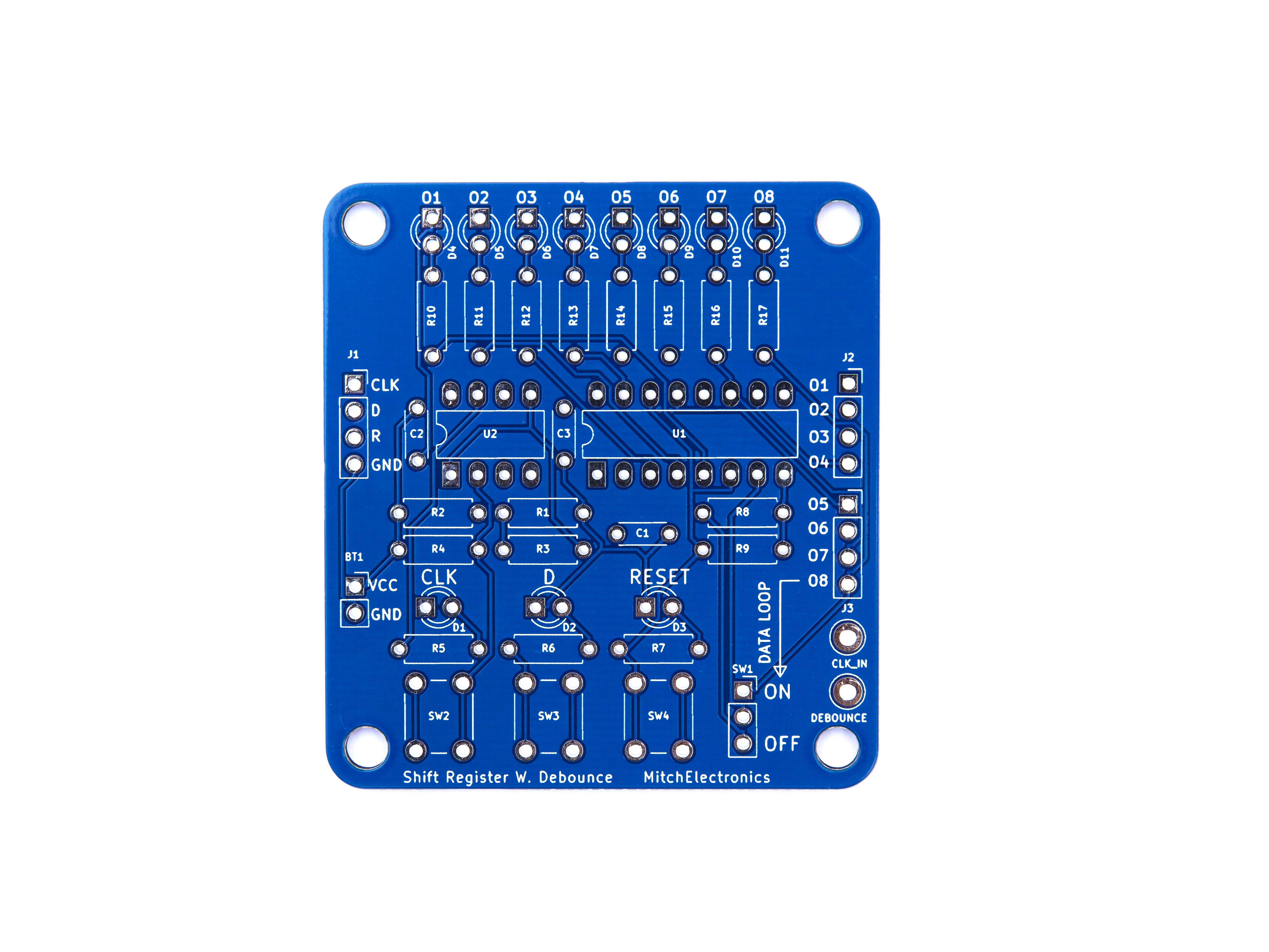
Before applying power
- Check every component against its PCB reference.
- Confirm the orientation of all polarised components and ICs.
- Inspect for solder bridges, unsoldered pads and clipped leads that could cause a short.
- Check that no loose wire or solder debris remains on the board.
Build with confidence
Construction tips
Recommended build order
A reliable way to assemble 4015 Shift Register Board is to work from the lowest-profile components to the tallest. This keeps the PCB easy to access while you solder.
- Fit resistors, links and other low-profile components first.
- Fit small capacitors and diodes, checking polarity where applicable.
- Fit IC sockets and small semiconductors, observing the orientation markings.
- Fit larger capacitors, potentiometers, switches and other controls.
- Fit LEDs, connectors and the remaining taller components.
- Insert socketed ICs only after soldering around the socket is complete.
- Inspect every joint and check for solder bridges before applying power.
Electronics construction guidance
If you are new to kit construction, use the Soldering Guide alongside these instructions. Identify each component before fitting it and compare its reference with the component list and PCB silkscreen.
When it does not work
Troubleshooting
Nothing happens when power is applied
- Confirm the supply is connected to the correct input and with the correct polarity.
- Check that ICs, diodes, LEDs, transistors and electrolytic capacitors are fitted in the correct orientation.
- Compare component values and positions against the component list and PCB reference.
- Inspect for missed joints, dry joints and accidental solder bridges.
The circuit powers up but does not behave as expected
This kit is intended for serial shift-register and digital logic experimentation. If the output is stuck, unstable or outside the expected behaviour, use the schematic to trace the circuit a stage at a time rather than replacing several parts at once.
Check the components around the part of the circuit responsible for the output or timing first. A misplaced resistor, reversed semiconductor or poor connection can allow a circuit to power up while preventing it from operating correctly.
The circuit works intermittently
Intermittent behaviour is often caused by a marginal solder joint, a loose connector or a component lead that has not been fully soldered. Gently inspect the board with power removed and reflow any joint that looks dull, cracked or incomplete.
If the fault remains, compare the assembled board with the schematic and PCB reference one connection at a time.
Ready to test and experiment?
Use a signal generator to test how fast the logic circuits can respond to signals
Once the board is working, compare its behaviour with the schematic and the explanation above. Try changing only one input, control or permitted component value at a time so you can clearly see what effect that change has on the circuit.